Probe cleaning method and probe cleaning device

A technology for cleaning devices and probes, applied in the field of probe cleaning and probe cleaning devices, can solve the problems that the accuracy and reliability of wafer test results need to be improved, and achieve the ability to prevent incomplete cleaning and remove impurities. , the effect of reducing cleaning time

Active Publication Date: 2014-06-25
SHANGHAI HUAHONG GRACE SEMICON MFG CORP
View PDF5 Cites 20 Cited by
  • Summary
  • Abstract
  • Description
  • Claims
  • Application Information

AI Technical Summary

Problems solved by technology

[0005] However, the accuracy and reliability of prior art wafer test results need to be improved

Method used


Image

  • Probe cleaning method and probe cleaning device
  • Probe cleaning method and probe cleaning device
  • Probe cleaning method and probe cleaning device

Examples


Embodiment Construction

[0029] It can be seen from the background art that the accuracy and authenticity of wafer testing in the prior art need to be improved.

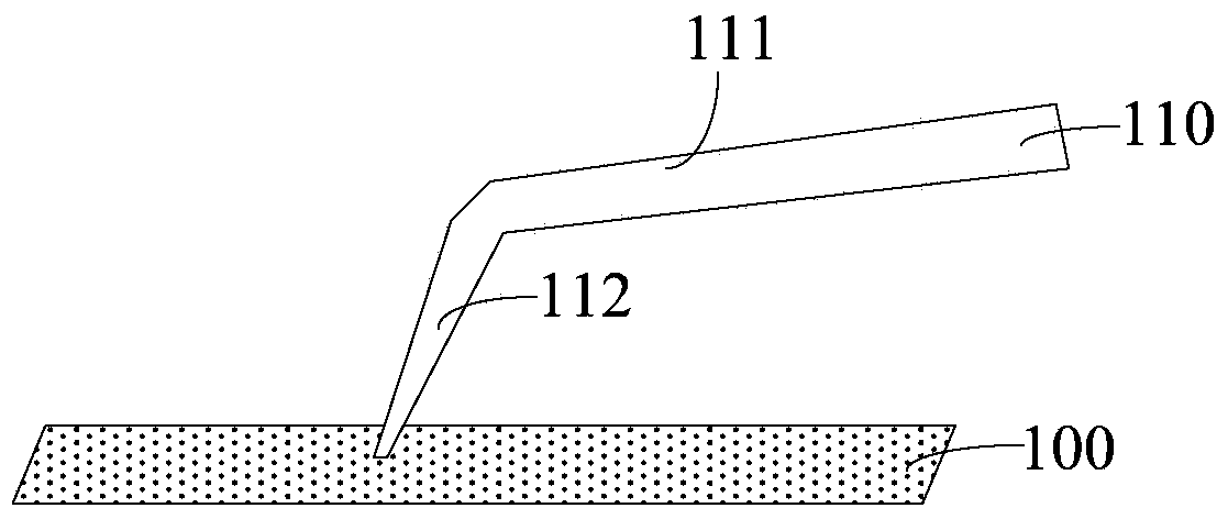
[0030] In order to solve the above problems, the analysis is carried out for wafer testing. Wafer testing has high accuracy in the electrical testing of the die, which is related to the production yield, cost and quality of the wafer. Because the surface of the tested die often forms an oxide film due to oxidation or pollution, or in order to avoid damage to the die to be tested, an isolation film is usually formed on the die for protection, and the isolation film is usually a poor conductor; If the isolation film at the die is not removed or is not removed cleanly during the test, the isolation film will hinder the contact and electrification effect between the probe and the wafer die to be tested, thereby affecting the accuracy and reliability of electrical testing.

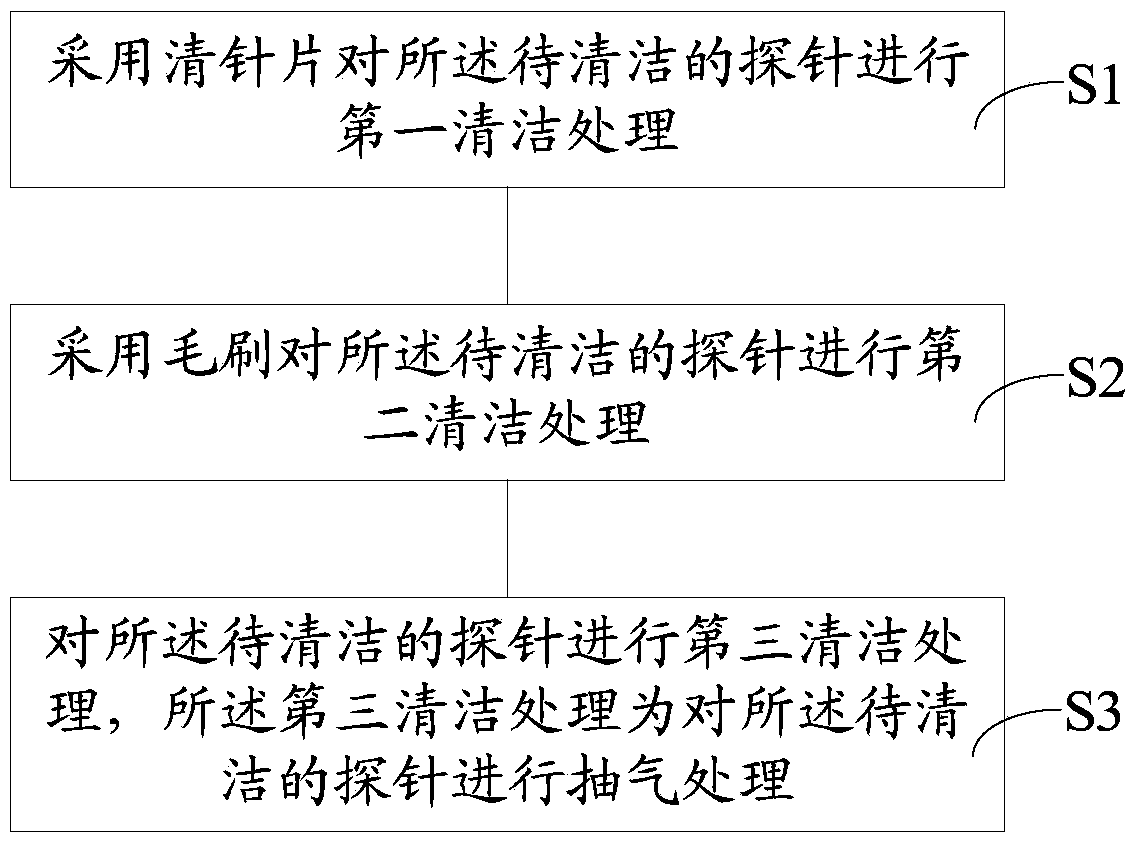
[0031] Therefore, when using a probe for electrical testing, a large co...


PUM


Abstract

The invention provides a probe cleaning method and a probe cleaning device. The probe cleaning method comprises the steps of providing a probe to be cleaned, adopting a probe cleaning piece to primarily clean the probe to be cleaned, adopting a brush to secondarily clean the probe to be cleaned, thirdly cleaning the probe to be cleaned, namely extracting air of the probe to be cleaned in the third cleaning process, and carrying out the first cleaning process, the second cleaning process and the third cleaning process at the same time. According to the probe cleaning method and the probe cleaning device, probe cleaning efficiency is improved, impurity removing ability is enhanced, probe cleaning time is shortened, accuracy and reliability of wafer testing results are improved, wafer testing time is shortened, and production efficiency is improved.

Description

technical field [0001] The invention relates to the technology in the field of semiconductor manufacturing, in particular to a probe cleaning method and a probe cleaning device. Background technique [0002] The entire manufacturing process of semiconductor devices can be divided into wafer manufacturing, wafer testing, wafer packaging, and final testing. [0003] The wafer manufacturing refers to manufacturing semiconductor devices on a wafer. After the semiconductor device is manufactured, a plurality of repeated dies will be formed on the wafer. In the wafer testing step, it is necessary to conduct an electrical test on the die to ensure that the die on the wafer is a qualified product before packaging, so wafer testing is one of the key steps to improve the yield of semiconductor devices . [0004] Generally, the test equipment includes a probe station (probe), and the probe station has a probe card (probe card), and the probe card includes at least one probe (probe ne...

Claims


Application Information

Patent Timeline
Patent Type & Authority Applications(China)
IPC IPC(8): B08B7/04
CPCB08B1/002B08B15/00
Inventor 王善屹
Owner SHANGHAI HUAHONG GRACE SEMICON MFG CORP
Why Eureka
Try Eureka