Automatic layout method for positions of heat through holes in 3D integrated circuit

An integrated circuit and automatic layout technology, applied in the direction of electrical digital data processing, special data processing applications, instruments, etc.

Inactive Publication Date: 2014-06-25
BEIJING UNIV OF TECH
View PDF3 Cites 8 Cited by
  • Summary
  • Abstract
  • Description
  • Claims
  • Application Information

AI Technical Summary

Problems solved by technology

Go through the en...

Method used


Image

  • Automatic layout method for positions of heat through holes in 3D integrated circuit
  • Automatic layout method for positions of heat through holes in 3D integrated circuit
  • Automatic layout method for positions of heat through holes in 3D integrated circuit

Examples


Embodiment Construction

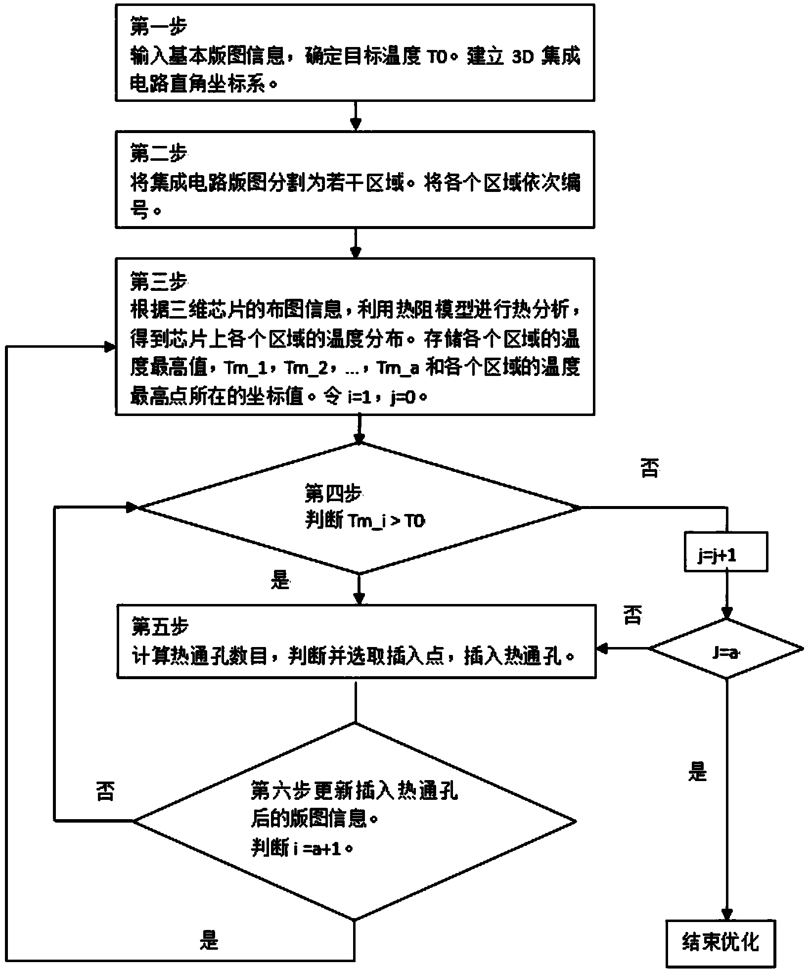
[0042] The present invention will be further described below in conjunction with the accompanying drawings.

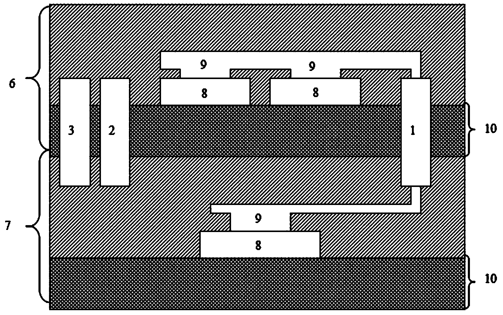
[0043] Such as figure 1 Shown is a schematic cross-sectional view of a 3D integrated circuit chip. The 3D integrated circuit in the present invention is a three-dimensional chip structure. figure 1 Among them, 1 is signal TSV, 2 is thermal via a, 3 is thermal via b, 6 is the top chip, 7 is the bottom chip, 8 is the chip standard unit, 9 is the metal connection layer, and 10 is the silicon substrate.

[0044] Each layer in the 3D chip is a 2D chip, and is connected vertically by the TSV shown in 1, which includes the top chip 6 and the low layer chip 7; the standard unit 8 is the basic component for realizing signal interconnection in the integrated circuit, Each standard unit 8 is interconnected through metal interconnection lines 9; the top chip 6 and the bottom chip 6 need to be connected through 1, 1. This TSV is a through-silicon hole passing through two adjacen...


PUM


Abstract

The invention relates to an automatic layout method for the positions of heat through holes in a 3D integrated circuit, belongs to the field of circuit design, and relates to a heat through hole inserting method for balancing a heat problem of the 3D integrated circuit. The automatic layout method for the positions of the heat through holes in the 3D integrated circuit comprises the steps that firstly, regional dividing and temperature analysis are carried out on a layout, and the number of the needed heat through holes and positions allowing the heat through holes to be inserted in are judged and calculated through a temperature comparison result; temperature analysis and judgment are carried out cyclically, and if temperature requirements are not met, the heat through holes are inserted until the temperature requirements are met by all regions. The whole automatic layout process is completed, the heat problem of the circuit is solved through the simple method, the original circuit structure is not damaged, the heat through holes are automatically inserted, process processing restraints are met by the heat through hole layout, and it is guaranteed that the temperature of all positions of a chip meets the temperature requirements.

Description

technical field [0001] The invention relates to a method for inserting a thermal via in a 3D integrated circuit, belongs to the field of circuit design, and relates to a method for inserting a thermal via to balance the heat problem of a 3D integrated circuit. Background technique [0002] With the rapid development of wireless communication, office electronics, entertainment electronics and other consumer electronics, integrated circuits have the characteristics of multi-function, miniaturization, portability, high speed, low power consumption and high reliability. Then, with the miniaturization of integrated circuits to the nanometer scale, how to continue to follow Moore's Law and how to realize a more miniaturized, diversified and low-cost system has become an urgent problem to be solved. These problems are accompanied by memory speed lag problems. Relative to processor speed, memory access speed has developed slowly, causing processor speed to stall while waiting for m...

Claims


Application Information

Patent Timeline
IPC IPC(8): G06F17/50
Inventor 侯立刚付婧妍汪金辉彭晓宏耿淑琴路博
Owner BEIJING UNIV OF TECH
Why Eureka
Try Eureka