

Making method for defect detection wafer used in polysilicon chemical mechanical grinding process
A technology of chemical machinery and grinding process, which is applied in semiconductor/solid-state device manufacturing, semiconductor/solid-state device testing/measurement, electrical components, etc., and can solve problems such as data interference of testers
- Summary
- Abstract
- Description
- Claims
- Application Information
AI Technical Summary
Problems solved by technology
Method used
Image

Examples
Embodiment Construction
[0019] based on the following figure 1 and figure 2 , specifically explain the preferred embodiment of the present invention.
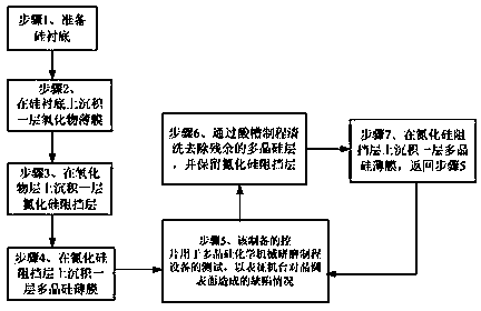
[0020] Such as figure 1 As shown, the present invention provides a method for manufacturing a wafer for defect detection in a polysilicon chemical mechanical polishing process, the method comprising the following steps:
[0021] Step 1, preparing the silicon substrate;
[0022] Step 2, depositing a layer of oxide film on the silicon substrate;
[0023] Step 3, depositing a silicon nitride barrier layer on the oxide layer;
[0024] Step 4, depositing a layer of polysilicon film on the silicon nitride barrier layer;
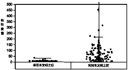
[0025] Step 5, the prepared control sheet is used for testing polysilicon chemical mechanical polishing process equipment to characterize the defects caused by the polishing process on the wafer surface;
[0026] Step 6, cleaning and removing the residual polysilicon layer through an acid bath process, and retaining the silicon nitr...
PUM
 Abstract
Description
Claims
Application Information