Method for Detecting Bridge Defects at the Bottom of Polysilicon Using Small Window Pattern Test Structure

A technology for testing structures and small windows, which is applied in semiconductor/solid-state device testing/measurement, measurement devices, material analysis using wave/particle radiation, etc. It can solve the problem that polysilicon gate etching residual defects are not easy to be detected, etc. , to achieve the effects of shortening the R&D cycle, guaranteeing product yield, and shortening the impact interval

Active Publication Date: 2017-01-04
SHANGHAI HUALI MICROELECTRONICS CORP
View PDF5 Cites 0 Cited by
  • Summary
  • Abstract
  • Description
  • Claims
  • Application Information

AI Technical Summary

Problems solved by technology

[0008] The present invention solves the problem that the etching residual defects of the polysilicon gate in the limit size are not easy to be detected, thereby providing a technical solution of a method for detecting bridging defects at the bottom of polysilicon by using a small window pattern test structure

Method used


Image

  • Method for Detecting Bridge Defects at the Bottom of Polysilicon Using Small Window Pattern Test Structure
  • Method for Detecting Bridge Defects at the Bottom of Polysilicon Using Small Window Pattern Test Structure
  • Method for Detecting Bridge Defects at the Bottom of Polysilicon Using Small Window Pattern Test Structure

Examples


Embodiment Construction

[0027] The present invention will be further described below in conjunction with the accompanying drawings and specific embodiments, but not as a limitation of the present invention.

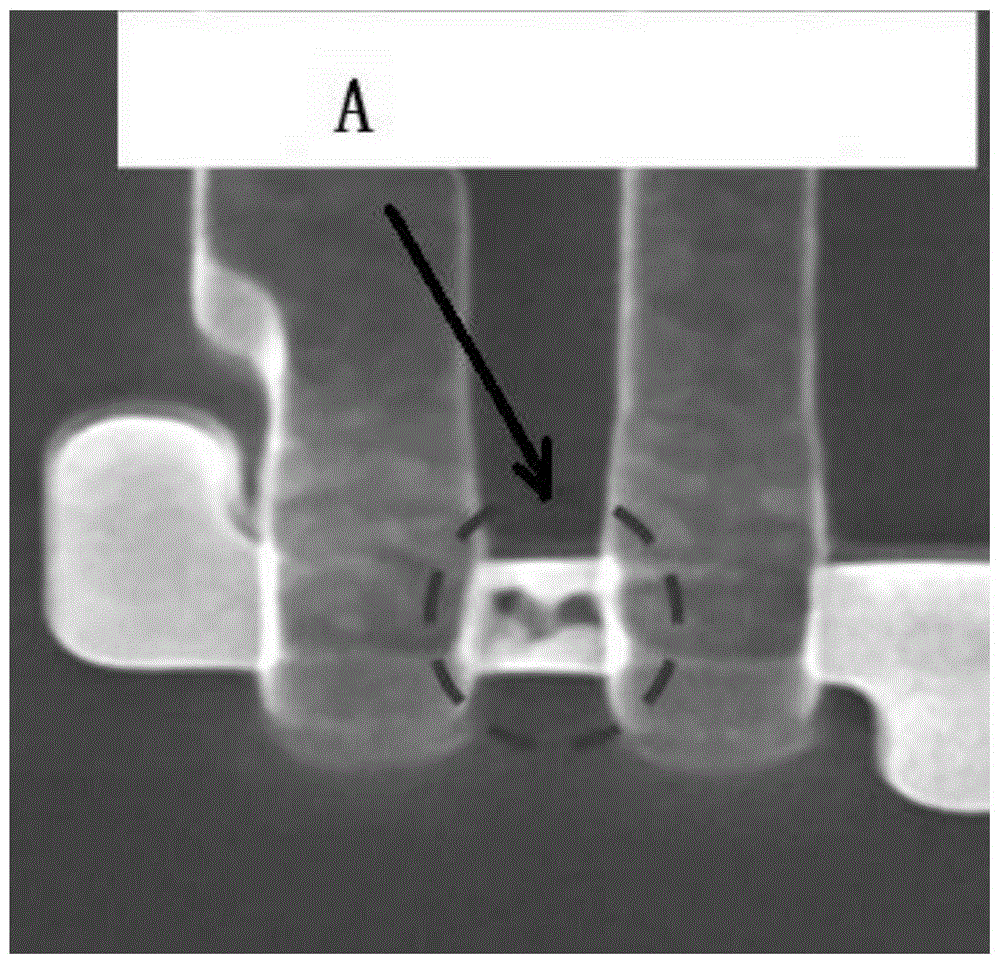
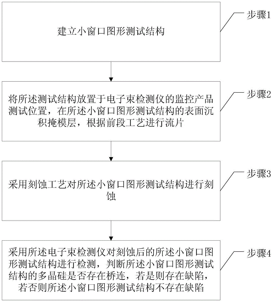
[0028] like figure 2 As shown, the present invention provides a method for detecting polysilicon bottom bridging 6 defects using a small window pattern test structure, comprising the following steps:

[0029] Take the 55nm logic product to establish a small window graphic test structure as an example:

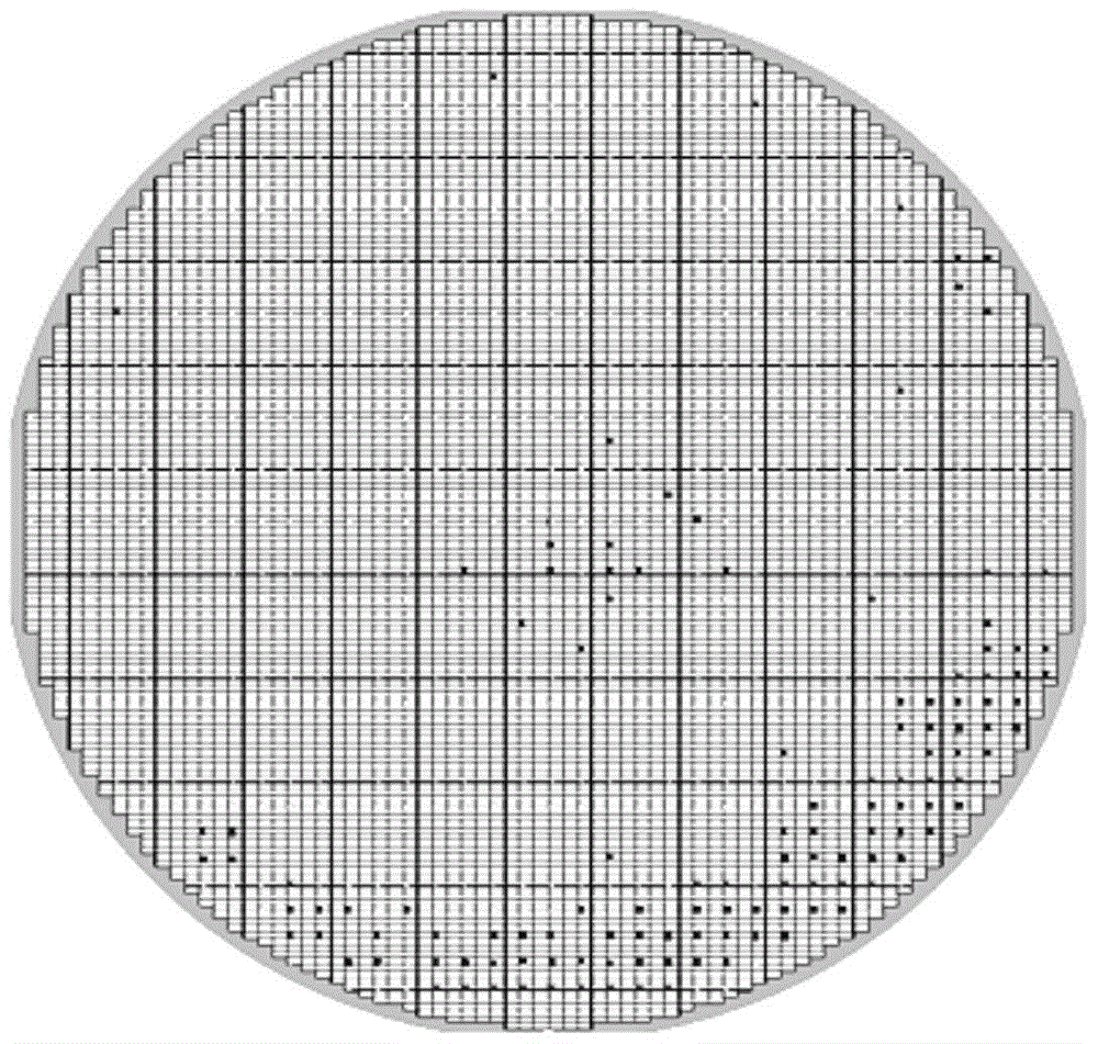
[0030] Step 1. Establish a small window pattern test structure (such as image 3 shown);

[0031] Step 2. Place the small window pattern test structure on the monitoring product test position of the electron beam detector, deposit a mask layer on the surface of the small window pattern test structure, and tape out according to the previous process;

[0032] Step 3. Etching the small window pattern test structure by an etching process;

[0033] Step 4. Adopt electron beam detector to detect t...


PUM


Abstract

The invention discloses a method for detecting a bridging defect on a polysilicon bottom by using a small window graph detection structure, relating to the circuit manufacture technology field. The method comprising steps of establishing a small window graph test structure, placing the test structure on a monitor product test position of an electron beam detection instrument, depositing a mask layer on the surface of the small window test graph structure and tapping out according to the previous technology, utilizing the etching technology to etch on the small window graph test structure, utilizing the electron beam detection instrument to detect the etched small window graph test structure, determining that whether the polysilicon of the small window graph test structure has bridging, if yes, the defect of the small window graph test structure exists, if not , the defect of the small window graph test structure does not exist. The method provided by the invention can discover the defect promptly, can provide data reference for improving yield during the process of research and development, can shorten the research and development cycle, can provide monitor means for products, can shorten influence interval and can provide guarantee for the yield of products.

Description

technical field [0001] The invention relates to the field of integrated circuit manufacturing technology, in particular to the detection of polysilicon etching defects. Background technique [0002] With the development of integrated circuit technology and the scaling down of critical dimensions, it is very important to detect defects of limit size online in time to improve the yield rate. For this reason, semiconductor manufacturing uses a variety of detection methods, such as: dark field scanning, bright field scanning And electron beam (E-beam) scanning, etc. However, not all defects can be detected. For example, the polysilicon gate etching residual defect A in the limit size is not easy to be detected, such as Figure 1a and Figure 1b shown. [0003] The reason is that the size and thickness of such defects are beyond the capability of optical detection, and there is no difference in voltage contrast. The difference between the secondary electron signal and the backg...

Claims


Application Information

Patent Timeline
Patent Type & Authority Patents(China)
IPC IPC(8): H01L21/66G01N23/00
CPCH01L22/12
Inventor 范荣伟刘秀勇龙吟倪棋梁陈宏璘
Owner SHANGHAI HUALI MICROELECTRONICS CORP
Why Eureka
Try Eureka