A pss patterned substrate etching method

A technology for patterning substrates and substrates, applied in the field of plasma, can solve the problems of decreased production efficiency, increased bottom width of PSS patterns, etc., and achieves the effects of suppressing bottom width, improving PSS etching process, and improving growth quality

Active Publication Date: 2016-08-31
BEIJING NAURA MICROELECTRONICS EQUIP CO LTD
View PDF5 Cites 1 Cited by
  • Summary
  • Abstract
  • Description
  • Claims
  • Application Information

AI Technical Summary

Problems solved by technology

[0008] The present invention provides a method for etching a PSS patterned substrate to at least solve one of the above technical problems, that is, to solve the problem caused by the method of increasing the etching ratio by reducing the power of the lower electrode in the PSS etching of the prior art. A large increase in the bottom width of PSS graphics and the resulting decrease in production efficiency

Method used


Image

  • A pss patterned substrate etching method
  • A pss patterned substrate etching method
  • A pss patterned substrate etching method

Examples


Embodiment Construction

[0040]In order to enable those skilled in the art to better understand the technical solution of the present invention, the method for etching a PSS patterned substrate provided by an embodiment of the present invention will be described in detail below with reference to the accompanying drawings.

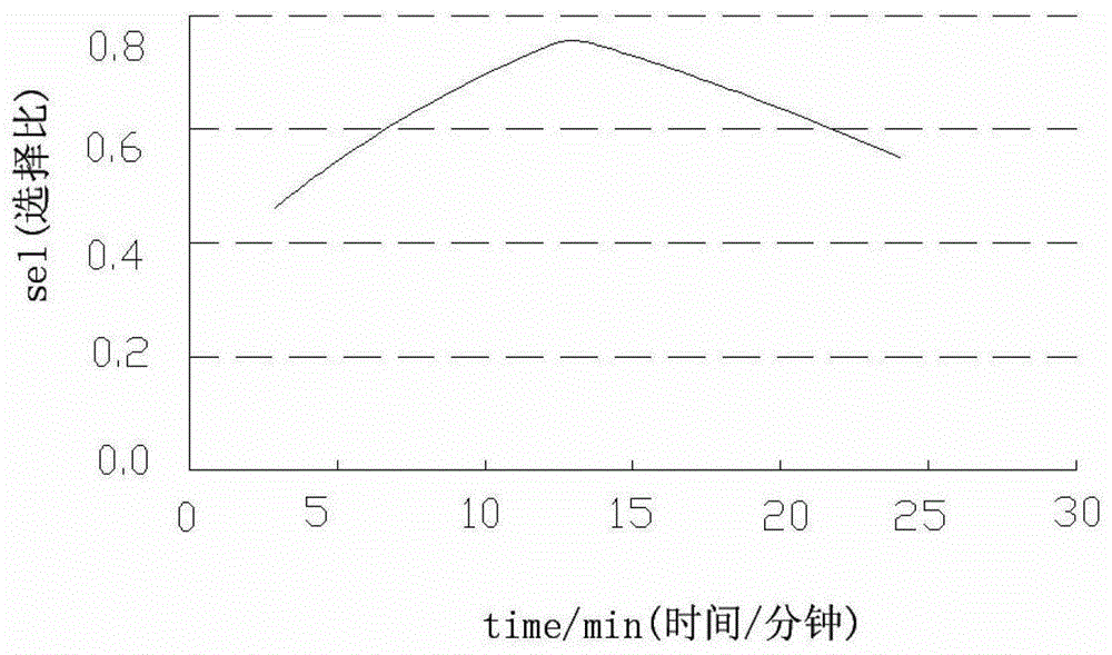
[0041] In order to suppress the widening of the bottom width of the PSS pattern in the PSS process, a set of experimental data on the change of the selection ratio and the bottom width in the etching process is provided in the embodiment of the present invention, and based on the experiment, the embodiment of the present invention proposes a A PSS patterned substrate etching method. see Figure 3A , which shows the change graph of the selectivity ratio during the main etching process, in Figure 3A Among them, the change of selectivity presents an increase first and then decrease, which is similar to a parabolic law, in which the turning point of selectivity from increase to decre...


PUM


Abstract

The invention provides a PSS (Patterned Sapphire Substrate) etching method. The method includes: providing the substrate and manufacturing a mask with a needed pattern on the substrate; etching the substrate according to a main etching process; etching the substrate according to an over etching process; and ending the etching. The main etching process includes N etching sub-processes and as for two adjacent etching sub-processes, a lower-electrode radio-frequency power adopted in the latter etching sub-process is higher than a lower-electrode radio-frequency power which is adopted by the former etching sub-process and N is an integer larger than or equal to 3. The PSS etching method provided by the embodiment of the invention inhibits a problem, which exists in the prior art, that a method which reduces the lower-electrode power causes a large increase of the bottom width of the PSS pattern and causes reduction of production efficiency so that the bottom width is effectively inhibited and a selection ratio of the whole main etching process is improved at the same time and the PSS etching process is improved and the growth quality of a GaN epitaxy is improved.

Description

technical field [0001] The invention relates to plasma technology, in particular to a PSS patterned substrate etching method. Background technique [0002] With the continuous progress of GaN-based light-emitting diode (Light Emitting Diode, LED) technology, especially the maturity of blue light-excited phosphor powder to emit yellow light and mix it into white light, daily lighting can be realized in a low-cost and long-life way. Governments of various countries have proposed solid-state lighting revolution plans, which have greatly promoted the rapid development of LED technology. GaN-based LEDs have extremely broad application prospects in image display, signal indication, lighting, and basic research due to their excellent characteristics such as long life, impact resistance, earthquake resistance, and high efficiency and energy saving. [0003] Due to the difficulty in preparing GaN single crystals, GaN-based LED devices are usually prepared on sapphire substrates. Th...

Claims


Application Information

Patent Timeline
Patent Type & Authority Patents(China)
IPC IPC(8): H01L33/00
CPCH01L33/0066H01L33/22
Inventor 刘海鹰
Owner BEIJING NAURA MICROELECTRONICS EQUIP CO LTD
Why Eureka
Try Eureka