Methods of dynamically controlling film microstructure formed in a microcrystalline layer

A microcrystalline silicon layer, dynamic technology, applied in chemical instruments and methods, coatings, crystal growth, etc., can solve the problems of undeveloped PV devices, insufficient film formation and crystallization rate, and reduced manufacturing yield

Inactive Publication Date: 2011-11-09
APPLIED MATERIALS INC
View PDF1 Cites 0 Cited by
  • Summary
  • Abstract
  • Description
  • Claims
  • Application Information

AI Technical Summary

Problems solved by technology

However, no manufacturable process capable of delivering PV devices at high deposition rates and high film quality with low manufacturing costs has yet been developed
For example, insufficient crystallinity of silicon film can cause insufficient film formation and crystalline fraction, thereby reducing the conversion efficiency of PV solar cells
In addition, the conventional deposition process of microcrystalline silicon film (μc-Si) has a slow deposition rate, which disadvantageously reduces the manufacturing yield and increases the manufacturing cost

Method used


Image

  • Methods of dynamically controlling film microstructure formed in a microcrystalline layer
  • Methods of dynamically controlling film microstructure formed in a microcrystalline layer
  • Methods of dynamically controlling film microstructure formed in a microcrystalline layer

Examples


Embodiment Construction

[0016] The present invention describes a method for depositing intrinsic microcrystalline silicon layers with high deposition rates and uniform crystallinity. In one embodiment, the intrinsic type microcrystalline silicon layer can be deposited by dynamically controlling the process parameters used during the deposition process, thereby dynamically controlling the film properties and microstructure formed in the final intrinsic type microcrystalline silicon layer. In one embodiment, the intrinsic microcrystalline silicon layer can be used in a multi-junction solar cell or a single-junction solar cell.

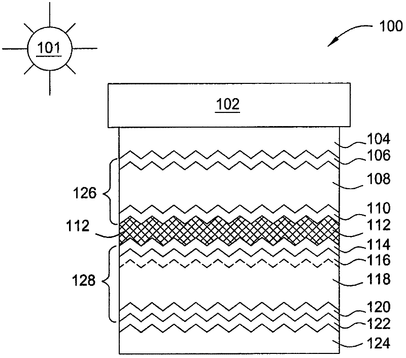
[0017] figure 1 is a schematic diagram of an embodiment of a multi-junction solar cell 100 oriented towards light or solar radiation 101 . The solar cell 100 includes a substrate 102, such as a glass substrate, a polymer substrate, a metal substrate, or other suitable substrate, over which a thin film is formed. The solar cell 100 also includes a first transparent conductive ...


PUM

PropertyMeasurementUnit
band gapaaaaaaaaaa

Abstract

A method for an intrinsic type microcrystalline silicon layer is provided. In one embodiment, a method for forming an intrinsic type microcrystalline silicon layer includes dynamically ramping up a silane gas supplied in a gas mixture to a surface of a substrate disposed in a processing chamber, dynamically ramping down a RF power applied in the gas mixture supplied to the processing chamber to form a plasma in the gas mixture, and forming an intrinsic type microcrystalline silicon layer on the substrate.

Description

technical field [0001] Embodiments of the invention generally relate to solar cells and methods of forming the same. More particularly, embodiments of the present invention relate to methods of forming microcrystalline silicon layers for solar applications. Background technique [0002] A photovoltaic device (PV) or solar cell is a device that converts sunlight into direct current (DC) electrical power. A PV or solar cell typically has one or more p-n junctions. Each junction consists of two distinct regions within the semiconductor material, one side denoted p-type region and the other side denoted n-type region. When the p-n junction of a PV cell is exposed to sunlight (consisting of photon energy), the sunlight is directly converted into electrical current through the PV effect. PV solar cells generate a specific amount of electrical power and the cells are tiled into modules sized to deliver the required amount of system power. PV modules are created by connecting mu...

Claims


Application Information

Patent Timeline
Patent Type & Authority Applications(China)
IPC IPC(8): C30B28/14C30B29/06C23C16/24C23C16/505H01L31/18H01L31/028
CPCC23C16/505Y02E10/50C30B29/06Y02E10/545C23C16/24C23C16/0272C23C16/52C30B25/105H01L31/076H01L31/1824Y02E10/548Y02E10/547Y02P70/50
Inventor 郑义宣广弛袁正布赖恩·赛
Owner APPLIED MATERIALS INC
Why Eureka
Try Eureka