Production method for type N ohm contact electrode of GaN based power type LED

An ohmic contact electrode, power-type technology, applied in circuits, electrical components, semiconductor devices, etc., can solve the problems of radio frequency damage to GaN substrates, poor thermal stability of N-GaN electrode alloy systems, etc.

Active Publication Date: 2009-02-11
YANGZHOU ZHONGKE SEMICON LIGHTING
View PDF4 Cites 0 Cited by
  • Summary
  • Abstract
  • Description
  • Claims
  • Application Information

AI Technical Summary

Problems solved by technology

[0004] The purpose of the present invention is to provide a method for preparing an N-type ohmic contact electrode of a GaN-based power LED, which improves the luminous efficiency of a GaN-based power LED and solves the problem of depositing SiO in PECVD. 2 Main technical problems such as radio frequency damage to the GaN substrate during the masking layer process, and poor thermal stability of the N-GaN electrode alloy system

Method used


Image

  • Production method for type N ohm contact electrode of GaN based power type LED
  • Production method for type N ohm contact electrode of GaN based power type LED
  • Production method for type N ohm contact electrode of GaN based power type LED

Examples


Embodiment Construction

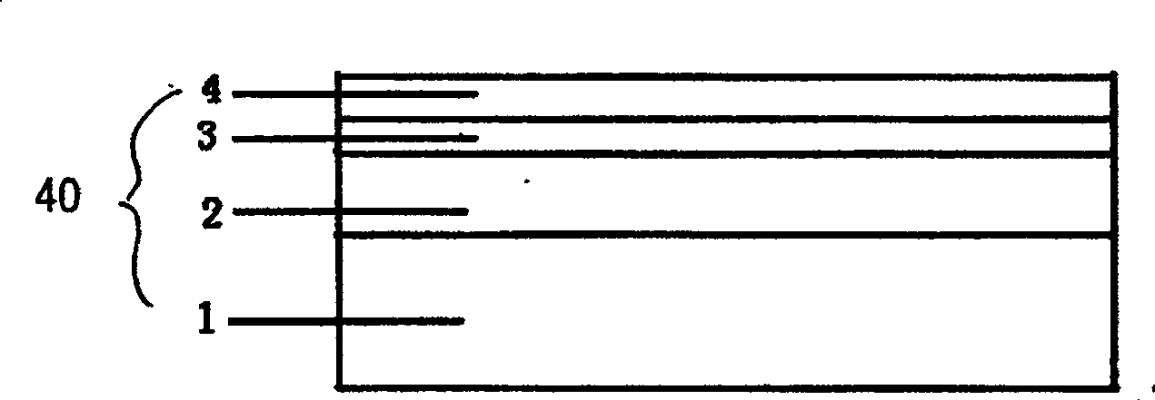
[0031] An N-type ohmic contact electrode for a GaN-based power LED and a preparation method thereof. The manufacturing process is generally to form an N-GaN layer 2, an active layer 3 and a P-GaN layer 4 on a sapphire substrate 1 by means of epitaxy , forming the material structure 40 of a GaN-based power LED, such as figure 1 shown.

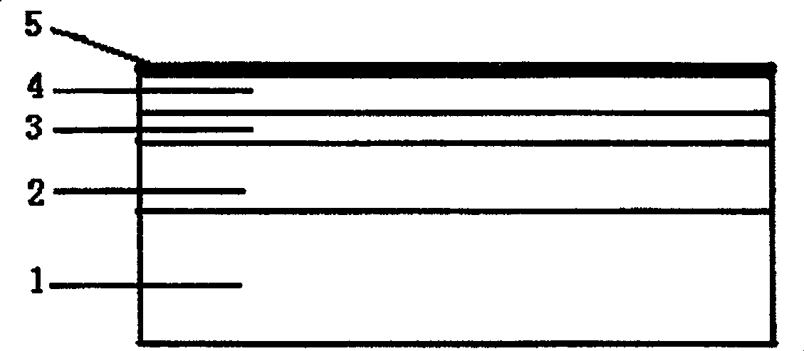
[0032] On the upper surface P-GaN layer 4 of the material structure (delete 40) of the epitaxial GaN-based power LED on the sapphire substrate 1, a layer of thickness 5000 is deposited by PECVD method. SiO 2 masking layer 5, such as figure 2 shown, where the PECVD-deposited SiO 2 Masking layer 5, evacuated to a pressure of less than 10 in the PECVD vacuum chamber -5 Pa, the temperature rises to 300°C and remains stable, the temperature is raised to 300°C in the vacuum chamber and remains stable, and the vacuum chamber is filled with N with a gas flow rate of 392 sccm 2 , 150sccm SiH 4 and 1420sccm N 2 O until the chamber pressure is 0.7...


PUM


Abstract

The present invention relates to a preparation method of an N-typed ohm contact electrode of the GaN basic-power-typed LED, which comprises a concealing layer that is deposited on the material structure of GaN basic-power-typed LED; an interdigital-shaped N-GaN electrode is eroded; the photosensitive resist is removed by washing; a separation layer is deposited on the surface of GaN substrate; an electrode is separated; SiO2 concealing layer is eroded; a P-GaN semi-transparent electrode metal system NiAu is prepared by the evaporation of the electronic beam; after the electrode is stripped off, and after the alloy with the ratio between N2 and O2 is 2 / 1is processed for five minutes at the temperature of 500 C DEG so as to reduce the ohm contact resistance between the metal system NiAu of P-GaN semi-transparent electrode and the P-GaN layer, and to improve the contact strength and the thermal stability of the P-GaN semi-transparent electrode and the P-GaN; finally a P-GaN thickened electrode is lithographic processed so as to complete the preparation of P and N electrode.

Description

technical field [0001] The invention is used in the technical field of manufacturing semiconductor optoelectronic devices, and in particular relates to a method for designing and manufacturing an N-GaN electrode system in a GaN-based power light-emitting diode (LED). Background technique [0002] Using InGaN / GaN MQW blue chip to excite yellow phosphor (YAG: Ce 3+ ) is the most commonly used method for preparing white light LEDs. White light LEDs have outstanding advantages such as energy saving, environmental protection, cold light source, high color rendering index, fast response speed, small size and long working life. With the in-depth research on InGaN / GaNMQW blue light materials and the steady improvement in the preparation performance of power-type white light LED devices, LEDs have moved from backlights, traffic lights, display signs, landscape lighting to white light lighting and other fields used in electronic products. Semiconductor solid-state lighting As a green...

Claims


Application Information

Patent Timeline
Patent Type & Authority Patents(China)
IPC IPC(8): H01L33/00H01L33/40
Inventor 陈宇王良臣伊晓燕郭金霞
Owner YANGZHOU ZHONGKE SEMICON LIGHTING
Why Eureka
Try Eureka