Heaters for plasma processing plants

A processing device and heater technology, which is applied in semiconductor/solid-state device manufacturing, electrical components, circuits, etc., can solve problems such as affecting the etching rate and etching uniformity, affecting the heating effect of the heating component 102, etc., so as to reduce power loss. , avoid influence, reduce the effect of coupling current

Active Publication Date: 2019-01-18
ADVANCED MICRO FAB EQUIP INC CHINA
View PDF3 Cites 0 Cited by
  • Summary
  • Abstract
  • Description
  • Claims
  • Application Information

AI Technical Summary

Problems solved by technology

Because r1 and r2 are equivalent resistances produced by capacitive coupling, the resistance value is much greater than the resistance R of the heating element 102, so the magnitude of the coupling current I has little to do with the resistance of the heating element 102, and the heat generated by the coupling current I 2 R will cause the ICP source power loss, so if you want to reduce the source power loss, you need to reduce the resistance value of R. However, reducing the resistance value of the heating element 102 will affect the heating effect of the heating element 102, affecting the etching rate and etching uniformity sex

Method used


Image

  • Heaters for plasma processing plants
  • Heaters for plasma processing plants
  • Heaters for plasma processing plants

Examples


Embodiment Construction

[0020] Specific embodiments of the present invention will be further described below in conjunction with the accompanying drawings.

[0021] The invention discloses a heater for a plasma processing device of inductively coupled plasma (ICP).

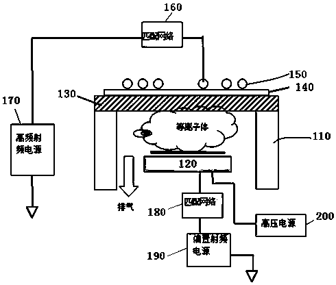
[0022] Such as figure 2 As shown, in an embodiment of an inductively coupled plasma plasma processing device, the plasma processing device includes an inductively coupled plasma reaction chamber (ICP chamber) 110, and the shape of the reaction chamber 110 is not limited to a cylindrical shape, for example It can also be horn-shaped.

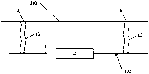
[0023] At the bottom of the reaction chamber 110, there is a support table 120 for placing wafers. The support table 120 can be provided with electrostatic chucks for absorbing wafers, electrodes, temperature modulation mechanisms such as heaters or refrigerant flow paths, etc. . During semiconductor processing, the inside of the processing chamber is filled with plasma.

[0024] The top of the reactio...


PUM


Abstract

The invention discloses a heater for a plasma processing device, and a plasma reactor comprises a reaction cavity. The top of the reaction cavity is provided with an insulating window, and the insulating window is sequentially provided with a heater and a coil. The heater comprises a metal shielding protection layer and a heating resistor layer. The metal shielding protection layer completely covers the heating resistor layer. The radio frequency emitted by the coil of the plasma processing device sequentially passes through the metal shielding protection layer and the heating resistor layer to enter the reaction cavity of the plasma processing device. The resistance of the metal shielding protection layer is less that the resistance of the electric heater. The heating resistor layer is covered by the metal shielding protection layer with the resistance being less than the impedance of the heating resistor layer. The metal shielding protection layer is used for replacing the heating resistor layer to achieve the capacitive coupling of radio frequency power of the coil. The low impedance of the metal shielding protection layer enables the radio frequency power to be reduced. Because a coupling current on the metal shielding protection layer is generated through the capacitive coupling, the power loss, caused by capacitive coupling, of the radio frequency power is reduced, and more impact on a magnetic field of a source power is prevented.

Description

technical field [0001] The invention relates to a semiconductor etching technology, in particular to a heater used on an inductively coupled plasma reaction chamber. Background technique [0002] The inductively coupled plasma (ICP) reaction chamber needs to maintain a constant temperature to provide a consistent etching rate and uniformity of wafer surface etching, and the heating of the chamber lid (chamber lid) is also very important link. [0003] At present, in the prior art, the heating method of the reaction chamber cover mainly adopts the resistance heating method, and a heater element (heater element) is arranged on the reaction chamber cover, and the heating element is energized to generate heat energy for heating. This heating method can provide Excellent heating capability, but the disadvantage is that it absorbs part of the source power of the inductively coupled plasma coil (ICPcoil), resulting in a significant reduction in coupling efficiency. [0004] Such ...

Claims


Application Information

Patent Timeline
Patent Type & Authority Patents(China)
IPC IPC(8): H01L21/67
Inventor 万磊梁洁倪图强
Owner ADVANCED MICRO FAB EQUIP INC CHINA
Why Eureka
Try Eureka