
A kind of micro-chip light-emitting diode and its production process

A technology for light-emitting diodes and production processes, applied in electrical components, electrical solid-state devices, circuits, etc., can solve problems such as reducing product reliability, susceptibility to uneven force, and overflowing glue, improving bonding strength and avoiding high defect rates. , the effect of high luminous efficiency

Active Publication Date: 2017-01-04
浙江古越龙山电子科技发展有限公司
View PDF5 Cites 0 Cited by
  • Summary
  • Abstract
  • Description
  • Claims
  • Application Information

AI Technical Summary

Problems solved by technology

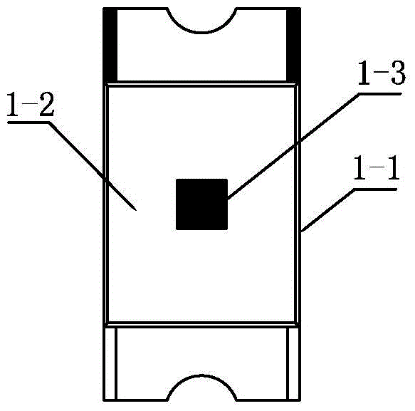
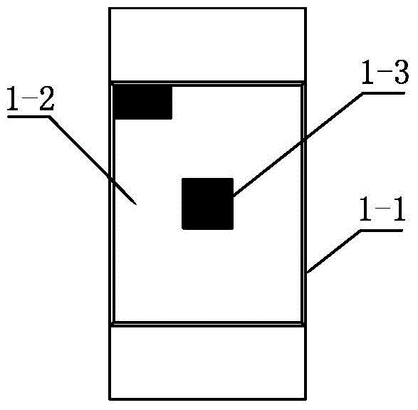
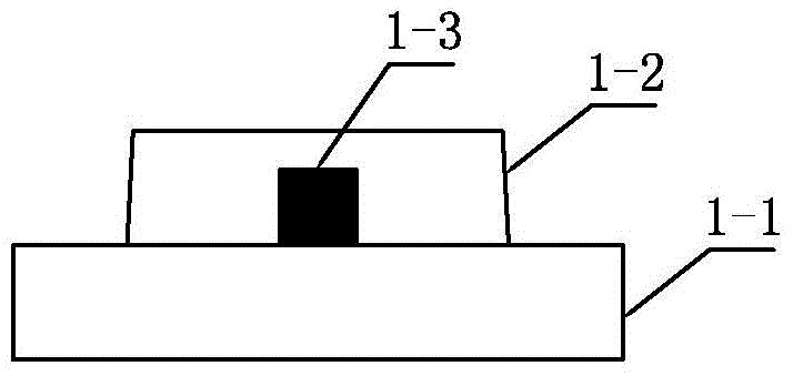
[0003] 1. The area of ​​colloid 1-2 only occupies a part of the entire product area, so that the luminous viewing angle is 120° and below, the entire luminous area of ​​the LED is insufficient, and the visual effect of luminescence is uneven; at the same time, in order to ensure sufficient luminous effect, only the entire SMD light-emitting diodes should be made as large as possible, resulting in a minimum of 1.6*0.8*0.4mm in the current market, and the production efficiency of single-chip products is low;
[0004] 2. The electrodes at both ends of the front are exposed to the air, which may easily cause oxidation of the pad or penetration of solder paste into the colloid along the conductive layer of the side wall of the light-emitting chip 1-3, affecting product quality and reducing product reliability; Area pads are easily affected by the environment and oxidized to cause poor soldering;
[0005] 3. The traditional packaging colloid process adopts strip packaging, which is prone to uneven force and overflow glue

Method used


Image

  • A kind of micro-chip light-emitting diode and its production process
  • A kind of micro-chip light-emitting diode and its production process
  • A kind of micro-chip light-emitting diode and its production process

Examples


Embodiment 1

[0043] Such as Figure 4-5As shown, a micro-chip light-emitting diode, including a substrate 1, a light-emitting chip 3 fixed on the substrate 1, and a colloid 2 covering the entire upper surface of the substrate 1, the via hole of the substrate 1 is filled with ink, The electrodes of the light-emitting chip 3 are connected to the substrate 1 through an arc-shaped wire 4. In this embodiment, the electrodes of the light-emitting chip 3 are located in the middle of the upper surface of the light-emitting chip 3. The beginning of the arc-shaped wire 4 is connected to the electrode of the light-emitting chip 3, and the end It is connected to the metal layer 12 of the substrate 1 by twice balling, and the distance between the highest point of the arc-shaped wire 4 and the surface electrode of the light-emitting chip 3 is 80 μm. The tail end of the arc-shaped wire 4 is welded by balling twice, which can strengthen the bonding strength between the arc-shaped wire 4 and the solder spo...

Embodiment 2

[0068] Such as Figure 4-5 As shown, a micro-chip light-emitting diode includes a substrate 1, a light-emitting chip 3 fixed on the substrate 1, and a colloid 2 covering the entire upper surface of the substrate 1, and the via hole of the substrate 1 is filled with resin. The electrodes of the light-emitting chip 3 are connected to the substrate 1 through an arc-shaped wire 4. In this embodiment, the electrodes of the light-emitting chip 3 are located in the middle of the upper surface of the light-emitting chip 3. The beginning of the arc-shaped wire 4 is connected to the electrode of the light-emitting chip 3, and the end It is connected to the metal layer 12 of the substrate 1 by twice balling, and the distance between the highest point of the arc-shaped wire 4 and the surface electrode of the light-emitting chip 3 is 100 μm. The tail end of the arc-shaped wire 4 is welded by balling twice, which can strengthen the bonding strength between the arc-shaped wire 4 and the sold...

Embodiment 3

[0073] Such as Figure 4-5 As shown, a micro-chip light-emitting diode, including a substrate 1, a light-emitting chip 3 fixed on the substrate 1, and a colloid 2 covering the entire upper surface of the substrate 1, the via hole of the substrate 1 is filled with ink, The electrodes of the light-emitting chip 3 are connected to the substrate 1 through an arc-shaped wire 4. In this embodiment, the electrodes of the light-emitting chip 3 are located in the middle of the upper surface of the light-emitting chip 3. The beginning of the arc-shaped wire 4 is connected to the electrode of the light-emitting chip 3, and the end It is connected to the metal layer 12 of the substrate 1 by twice balling, and the distance between the highest point of the arc-shaped wire 4 and the surface electrode of the light-emitting chip 3 is 130 μm. The tail end of the arc-shaped wire 4 is welded by balling twice, which can strengthen the bonding strength between the arc-shaped wire 4 and the solder s...


PUM


Abstract

The invention discloses a micro patch light-emitting diode and a production process thereof, belonging to the technical field of LEDs. The micro-chip light-emitting diode includes a substrate, a light-emitting chip fixed on the substrate, and a colloid covering the entire upper surface of the substrate. The via holes of the substrate are filled with ink or resin, and the electrodes of the light-emitting chip pass through arcs. The wires are connected to the substrate, and the length of the micro patch LED is 1.2-0.8 mm, the width is 1.0-0.5 mm, and the thickness is 0.4-0.6 mm. The micro-chip light-emitting diode production process includes the steps of solid crystal, wire bonding, compression molding, cutting, testing and packaging. The micro-chip light-emitting diode produced by the above process has small volume, high luminous efficiency, high brightness, and reliable performance. Features.

Description

technical field [0001] The invention relates to a miniature chip light-emitting diode and a production process thereof, belonging to the technical field of LEDs. Background technique [0002] The traditional SMD light-emitting diode (SMD LED) product structure can be divided into two types: through-hole type and straight-edge type, such as Figure 1-3 shown. Whether it is a through-hole type or a straight-edge type, the light-emitting chip 1-3 is packaged on the substrate 1-1 through the colloid 1-2. Generally, the area of ​​the colloid 1-2 only accounts for 2 / of the entire product area (that is, the area of ​​the substrate 1-1). 3. Even smaller, the electrodes and pads on both sides will be exposed outside the colloid 1-2, that is, the real light emitting area of ​​the whole product is only the part of the colloid 1-2. In addition, in order to ensure that the back pad and the front electrode of the traditional SMD light-emitting diode can still be connected after cutting,...

Claims


Application Information

Patent Timeline
Patent Type & Authority Patents(China)
IPC IPC(8): H01L33/48H01L33/62
CPCH01L2224/48091H01L2224/48227
Inventor 丁申冬陈丹萍宋晓明王利君王惠菊
Owner 浙江古越龙山电子科技发展有限公司
Learn More