Method for severing a semiconductor component assemblage

A technology for semiconductor and composite parts, which is applied in the field of dividing semiconductor device composite parts and can solve problems such as damage to semiconductor chips

Inactive Publication Date: 2014-06-25
OSRAM OPTO SEMICONDUCTORS GMBH
View PDF7 Cites 13 Cited by
  • Summary
  • Abstract
  • Description
  • Claims
  • Application Information

AI Technical Summary

Problems solved by technology

Such materials can cause the soldering material to spread over the separation surfaces

Method used


Image

  • Method for severing a semiconductor component assemblage
  • Method for severing a semiconductor component assemblage
  • Method for severing a semiconductor component assemblage

Examples


Embodiment Construction

[0029] Elements that are the same, of the same type or having the same function are provided with the same reference signs in the drawings.

[0030] The drawings and the size ratio of the elements shown in the drawings to each other cannot be regarded as to scale. More precisely, for better visibility and / or for better understanding, individual elements can be shown exaggerated.

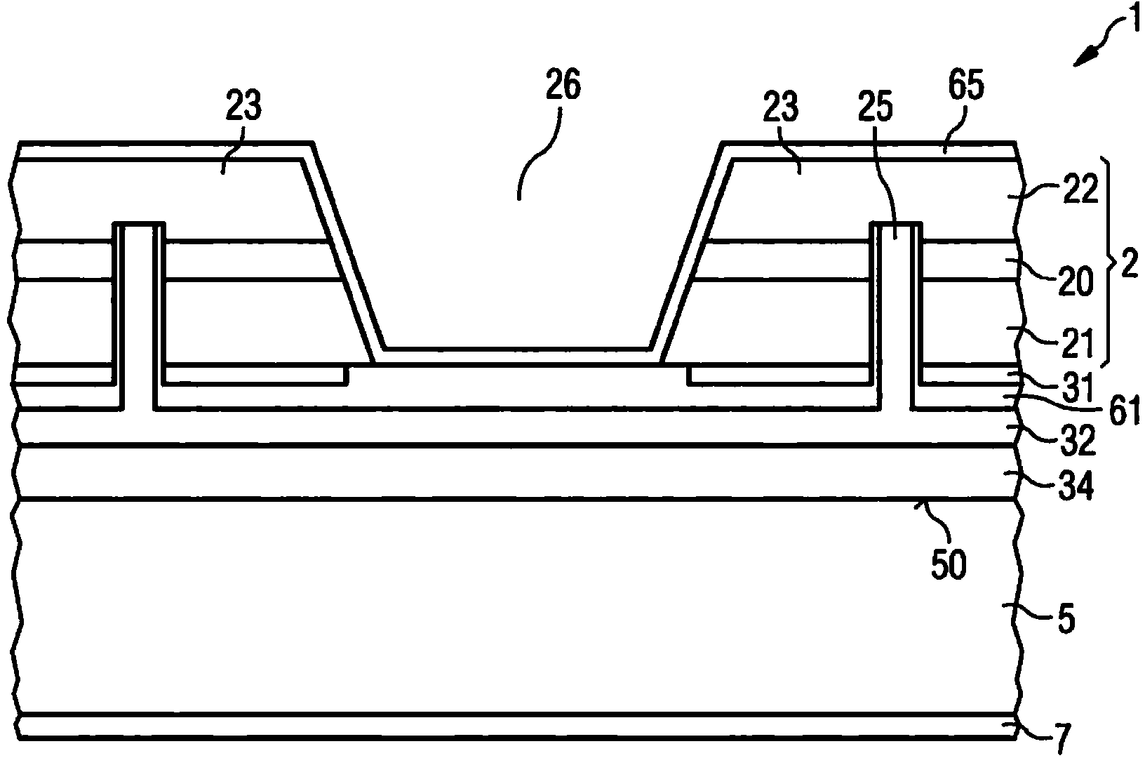
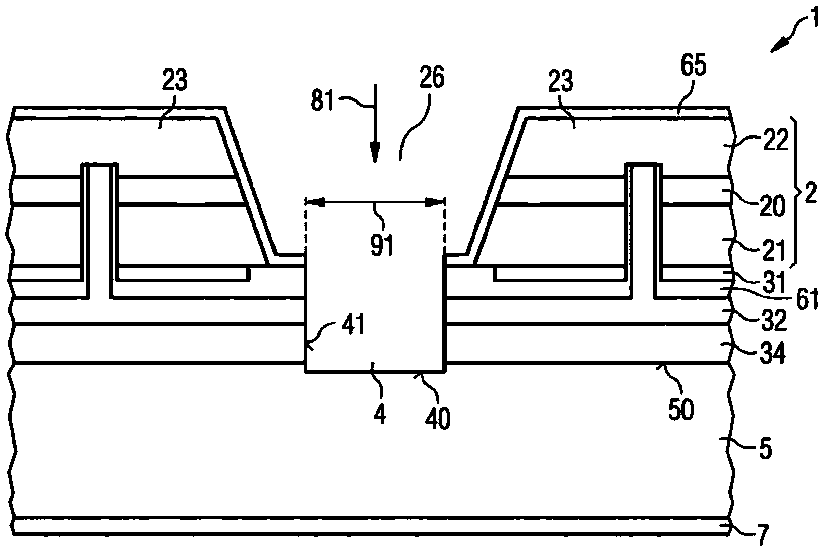
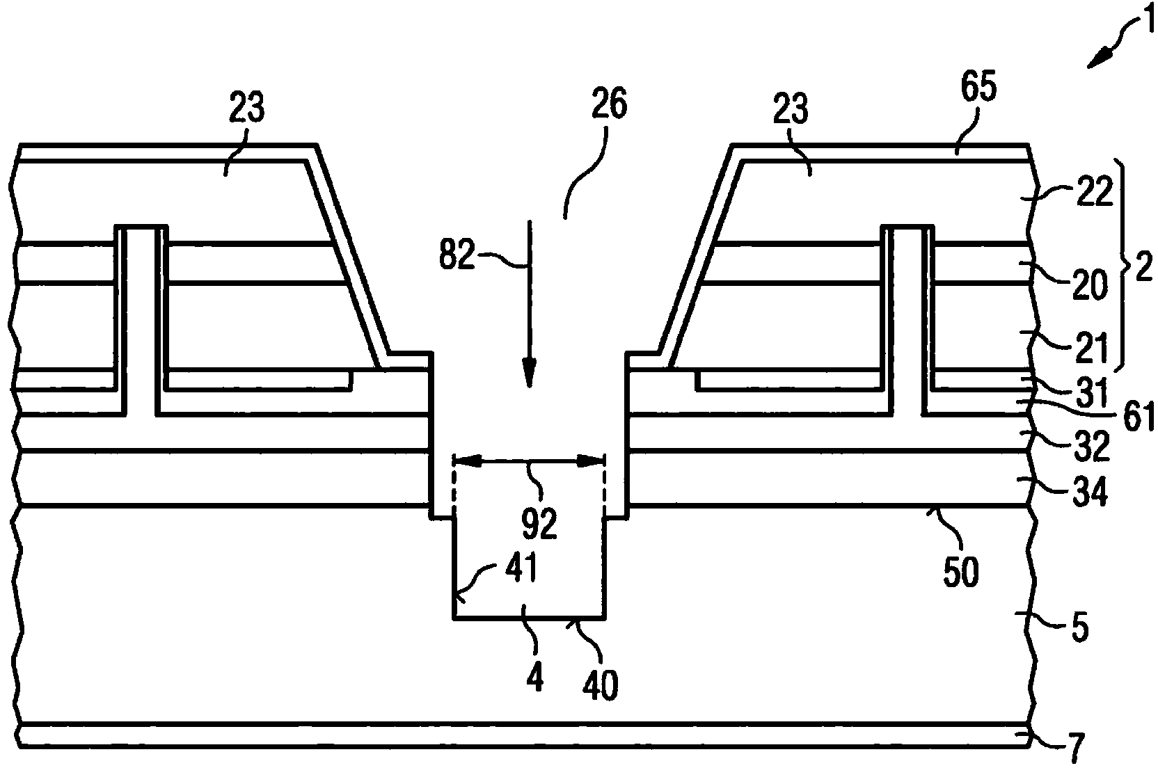
[0031] in Figure 1 to 5 A schematic cross-sectional view of a part of the semiconductor device composite 1 is shown in each. The method is described by way of example with the aid of the following semiconductor device assembly from which an optoelectronic semiconductor chip, in particular a light-emitting diode chip, is obtained during separation.

[0032] The semiconductor component assembly 1 has a carrier 5 with a main surface 50. The semiconductor layer sequence 2 is arranged on the main surface. The semiconductor layer sequence has an active area 20 provided for generating radiation. The active reg...


PUM

PropertyMeasurementUnit
Thicknessaaaaaaaaaa

Abstract

A description is given of a method for severing a semiconductor component assemblage (1) comprising a carrier (5) having a main face (50) and a semiconductor layer sequence (2) arranged on the main face. By means of a first laser cut, a separating trench (4) is formed in the semiconductor component assemblage (1), wherein the separating trench (4) only partly severs the semiconductor component assemblage (1) in a vertical direction running perpendicularly to the main face (50). The semiconductor component assemblage (1) is completely severed along the separating trench (4) with a severing cut by means of a laser.

Description

Technical field [0001] This application relates to a method for dividing a composite of semiconductor devices. Background technique [0002] In order to separate semiconductor chips from semiconductor wafers or wafer composites, laser separation methods can be used. It has been confirmed that the residue generated during the method can cover the separation surface. This material can cause the soldering material to be distributed on the separation surface when soldering the semiconductor chip and cause damage to the semiconductor chip. Summary of the invention [0003] One object is to propose a simple and reliable method for dividing a semiconductor device composite, in which the separated semiconductor chips can be reliably soldered. [0004] The objective is achieved by a method having the characteristics of claim 1. Design solutions and improvements are the subject of the dependent claims. [0005] In an embodiment of the method for dividing a semiconductor device assembly, the...

Claims


Application Information

Patent Timeline
IPC IPC(8): B23K26/38B23K26/402B23K26/40H01L33/00H01L33/38B23K26/364
CPCB23K26/38H01L21/78H01L33/382B23K26/409B23K26/367B23K26/4075H01L33/0095B23K2103/50B23K2103/172B23K26/40B23K26/364H01L21/3043H01L21/6835H01L2221/68327
Inventor 吉多·韦斯艾伯特·配希塔莱尔
Owner OSRAM OPTO SEMICONDUCTORS GMBH
Why Eureka
Try Eureka