Overall wiring method for super-large-scale integrated circuit under X structure

A large-scale integrated circuit and overall wiring technology, which is applied in the direction of electrical digital data processing, special data processing applications, instruments, etc., can solve the problem of less research on the overall wiring work of non-Manhattan structures, and achieve the goal of eliminating deviations and overcoming dependencies Effect

Active Publication Date: 2014-07-02
FUZHOU UNIV
View PDF2 Cites 25 Cited by
  • Summary
  • Abstract
  • Description
  • Claims
  • Application Information

AI Technical Summary

Problems solved by technology

However, there are few studies on the overall layout work of non-Manhattan st...

Method used


Image

  • Overall wiring method for super-large-scale integrated circuit under X structure
  • Overall wiring method for super-large-scale integrated circuit under X structure
  • Overall wiring method for super-large-scale integrated circuit under X structure

Examples


Embodiment Construction

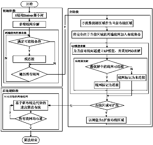
[0028] The VLSI overall wiring method under the X structure of the present invention, such as figure 1 shown, including the following steps:

[0029] (1) In the initial stage, use the Steiner minimum tree method to decompose the multi-terminal network into multiple two-terminal network, and connect the connectable two-terminal network with X-structure edge, that is, perform initial wiring, and obtain an approximate distribution of wiring congestion.

[0030] (2) In the main stage, select the most congested area from the approximate initial routing results as the current routing area, construct an integer linear programming model for the current routing area and use the improved particle swarm optimization method to solve it; then continuously expand the routing area and sequentially Solve until the routing area expands to the entire chip.

[0031] The improved particle swarm optimization method uses 0-1 sequence to encode, and imposes certain punishment on the scheme that vi...


PUM


Abstract

The invention relates to an overall wiring method for a super-large-scale integrated circuit under an X structure. The overall wiring method comprises the following steps of an initial stage: discomposing a multi-terminal wire network into a plurality of two-terminal wire networks by using a Steiner minimum tree method, and performing side connection on connectable two-terminal wire networks by using the X structure, namely performing initial wiring to obtain approximate wiring crowded distribution conditions; a main stage: selecting the most crowded area from the approximate initial wiring result as a current wiring area, establishing an integral linear programming model for the current wiring area, solving the integral linear programming model, continuously expanding the wiring area, and sequentially solving the wiring area until the wiring area is expanded to a whole chip; and an aftertreatment stage: redefining wiring side cost, and performing wiring on the two-terminal wire networks which are not communicated to one another by using a labyrinth algorithm based on the wiring side cost so as to obtain the final overall wiring result. By using the overall wiring method, the quality of a wiring scheme can be improved; and the overall wiring method is easy to implement, and is high in using effect.

Description

technical field [0001] The invention belongs to the technical field of integrated circuit computer aided design, and in particular relates to a high-quality X-structure overall wiring method in the field of ultra-large-scale integrated circuit wiring design. Background technique [0002] As the size of semiconductors and interconnects continues to shrink, more and more critical design metrics (such as wire length, latency, power consumption, etc.) are heavily impacted by interconnects. The routing stage, which is the actual wiring position of the organization interconnection lines, has become particularly important in the physical design of VLSI today. The complex routing process is composed of two stages: overall routing and detailed routing. In general routing, the routing of each net is assigned to each channel routing area, and the routing problems of each channel area are clearly defined. The detailed routing gives the specific location of each net in the channel area...

Claims


Application Information

Patent Timeline
IPC IPC(8): G06F17/50
Inventor 陈国龙郭文忠刘耿耿
Owner FUZHOU UNIV
Why Eureka
Try Eureka