Liquid crystal display with anti-static structure and manufacturing method thereof

A technology of liquid crystal display and manufacturing method, which is applied in the direction of instruments, nonlinear optics, optics, etc., and can solve the problems of increasing the conductive film and decreasing the transmittance of the panel

Active Publication Date: 2014-07-09
XIAMEN TIANMA MICRO ELECTRONICS
View PDF9 Cites 15 Cited by
  • Summary
  • Abstract
  • Description
  • Claims
  • Application Information

AI Technical Summary

Problems solved by technology

The smaller the resistance of the conductive film 4, the stronger the electrostatic protection ability, but to achieve a smaller resistance, the film thickness of the conductive film should be increased accordingly, which will lead to a decrease in the overall penetration rate of the panel

Method used


Image

  • Liquid crystal display with anti-static structure and manufacturing method thereof
  • Liquid crystal display with anti-static structure and manufacturing method thereof
  • Liquid crystal display with anti-static structure and manufacturing method thereof

Examples


specific Embodiment 1

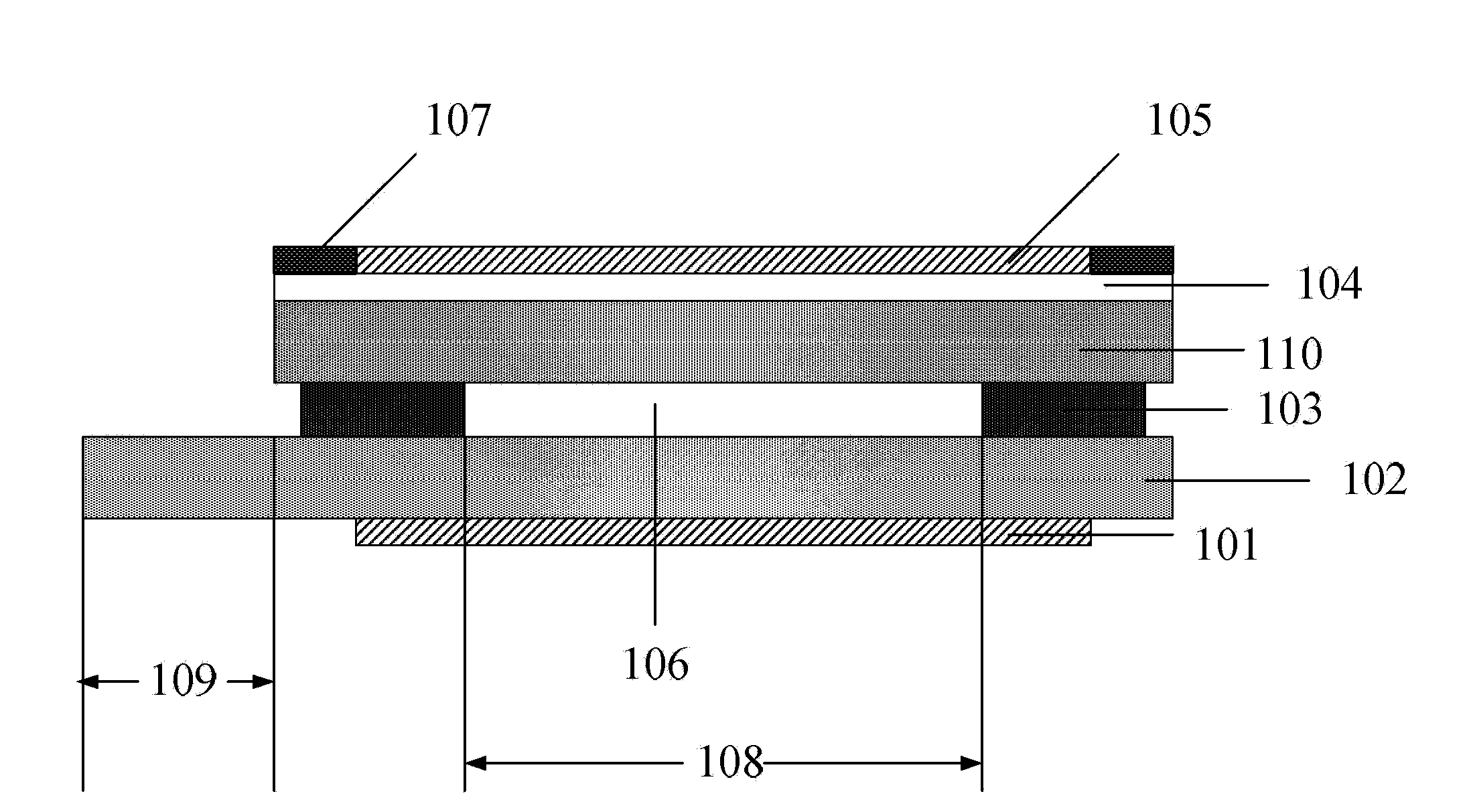
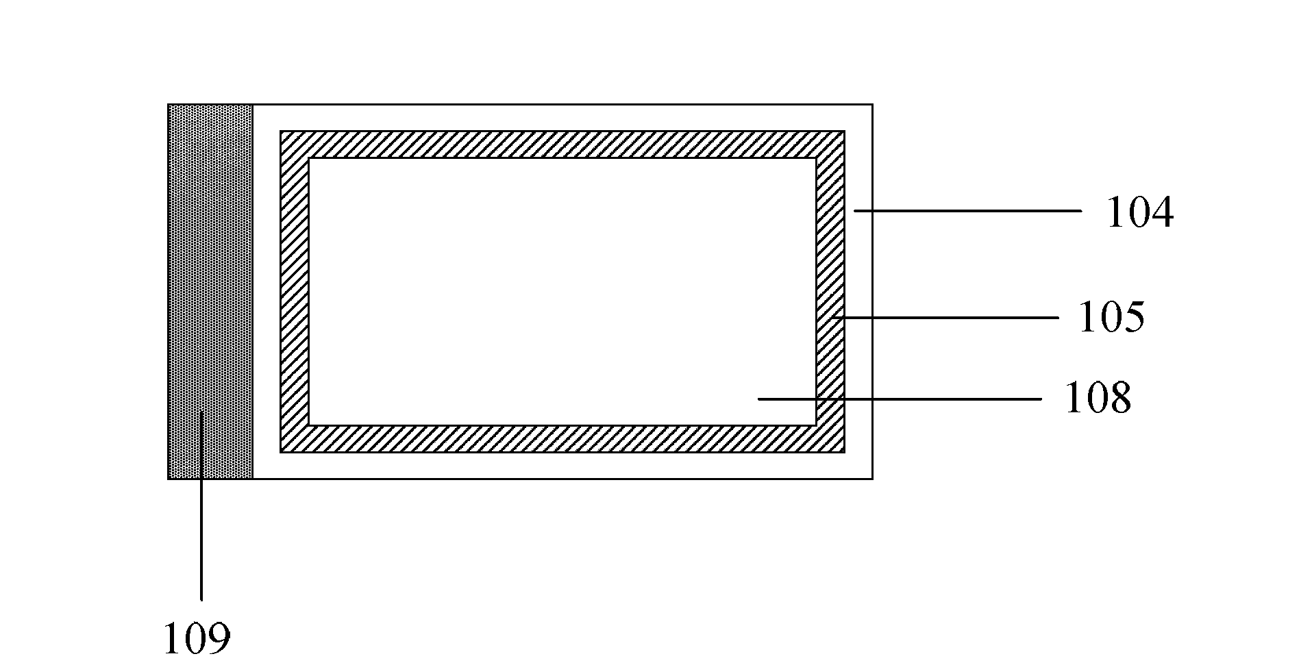
[0060] This embodiment provides a liquid crystal display with an antistatic structure, figure 2 A schematic diagram of the structure of the liquid crystal display. Such as figure 2 As shown, the liquid crystal display includes a color filter substrate 110 and an array substrate 102 arranged parallel to and corresponding to each other on the upper and lower sides, a liquid crystal layer 106 and a sealant 103 sandwiched between the color filter substrate 110 and the array substrate 102, the liquid crystal display Active display area 108 is included. There is a lower polarizer 101 under the array substrate, an upper polarizer 105 is arranged on the color filter substrate 110, and a first conductive film 104 is arranged between the upper polarizer 105 and the color filter substrate 110, and the first conductive film 104 It completely covers the color filter substrate 110 for electrostatic protection and electric field shielding. However, the first conductive film will reduce ...

specific Embodiment 2

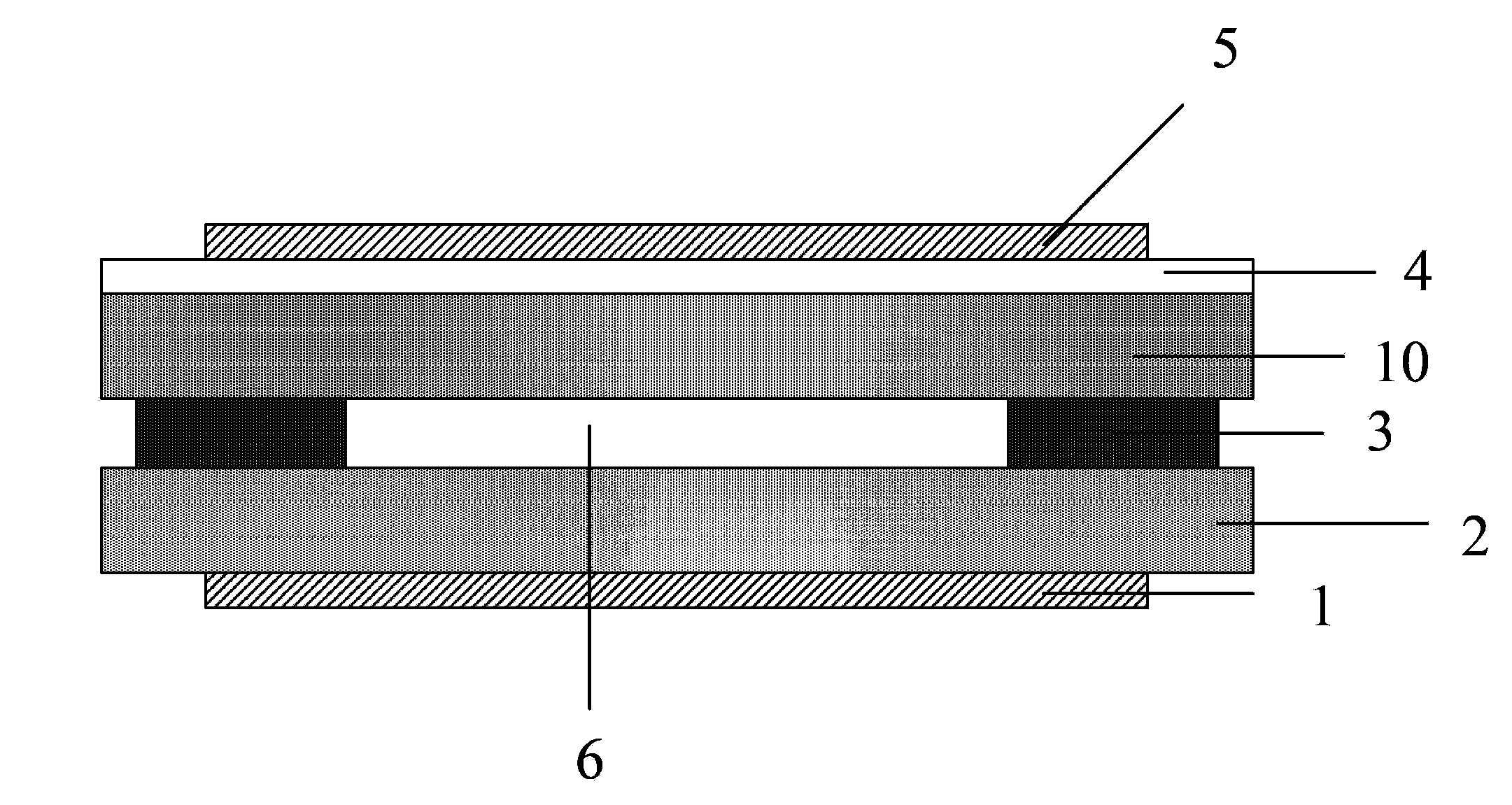
[0074] This embodiment provides another liquid crystal display with an antistatic structure, image 3 A schematic diagram of the structure of the liquid crystal display. Such as Figure 4 As shown, the liquid crystal display includes a color filter substrate 210 and an array substrate 202 arranged parallel to each other on the upper and lower sides, a liquid crystal molecular layer 206 and a sealant 203 sandwiched between the color filter substrate 210 and the array substrate 202, and the liquid crystal The molecular layer 206 forms the active display area 208 of the liquid crystal display.

[0075] There is a lower polarizer 201 under the array substrate, an upper polarizer 205 is arranged on the color filter substrate 210, and a layer of first conductive film 204 is provided between the upper polarizer 105 and the color filter substrate 210. The first conductive film 204 It completely covers the color filter substrate 210 for electrostatic protection and electric field shi...


PUM


Abstract

The invention discloses a liquid crystal display with an anti-static structure and a manufacturing method thereof. The liquid crystal display with the anti-static structure comprises a thin film transistor substrate, a lower polaroid which is arranged under the thin film transistor substrate, a color film substrate, a first conducting film which is arranged above the color film substrate, an upper polaroid which is arranged above the conducting film and liquid crystal molecules and sealing compound which are clamped between the thin film transistor substrate and a color film; the area of the upper polaroid is less than that of the first conducting film; an area on the first conducting film, which is not covered by the upper polaroid is provided with a second conducting film. The liquid crystal display with the anti-static structure has the advantages of enhancing the anti-static capability of the liquid crystal display, thinning the thickness of the conducting film which is accumulated on the color film substrate and accordingly maintaining or improving the penetration rate of the panel.

Description

technical field [0001] The invention relates to the technical field of liquid crystal displays, in particular to a liquid crystal display with an antistatic structure and a manufacturing method thereof. Background technique [0002] With the development of information technology, liquid crystal displays have been widely used in various aspects of information science. At the same time, higher requirements have been put forward for liquid crystal displays. Some products have particularly high requirements for antistatic. When the voltage applied to the liquid crystal cell is removed, due to electrostatic induction, the electric field in the liquid crystal cell fails to disappear instantly, and some pixels are still in the display state, which lasts for a while before disappearing. At present, many manufacturers add some antistatic agents to the liquid crystal to reduce the residual time of static electricity, but this method also reduces the reliability of the liquid crystal d...

Claims


Application Information

Patent Timeline
Patent Type & Authority Applications(China)
IPC IPC(8): G02F1/1335G02F1/1333
Inventor 林嘉民李俊谊
Owner XIAMEN TIANMA MICRO ELECTRONICS
Why Eureka
Try Eureka