Monolithic glass capacitive touch screen structure and processing method thereof

A technology of capacitive touch screen and monolithic glass, which is applied in the field of capacitive screen, can solve the problems of high processing cost, low light transmittance of G+P structure, heavy product weight, etc., and achieve the effect of high processing cost

Inactive Publication Date: 2014-07-09
SHENZHEN SANXIN JMT GLASS
View PDF7 Cites 2 Cited by
  • Summary
  • Abstract
  • Description
  • Claims
  • Application Information

AI Technical Summary

Problems solved by technology

[0003] The G+G structure is a double-layer glass structure of tempered glass + sensor glass. Due to the use of double-layer glass in this structure, the weight of the product is heavier and the thickness is thicker. higher;
[0004] The G+F structure is a structure of tempered glass + FILM film. Due to the low light transmittance of the FILM material, it affects the light transmittance of the touch screen, resulting in poor imaging effect, and requires the use of bonding technology during processing, which has a high Processing costs;
[0005] The G+P structure is the structure of the sensor glass + PET plastic sheet. Due to the low light transmittance of the PET material, the light transmittance of the G+P structure is relatively low, which affects the overall display effect of the touch screen;
[0006] Although the OGS structure is superior to the G+G structure, G+F structure, and G+P structure in terms of thickness, weight, light transmittance, and cost, but because OGS is a single-layer ITO structure, the single-layer ITO structure determines the ITO route. The length of the line, when the ITO line is long, the line resistance is high, it is difficult to meet the low line resistance requirements of the touch chip for the ITO line, so this structure is only suitable for touch screens below 10 inches, and cannot be applied to 10-32 inches and other large-size touch screens
[0007] Combining the above points, it can be seen that the existing capacitive touch screens are difficult to meet the requirements of large size, low cost, high light transmittance, thin thickness, and light weight.

Method used


Image

  • Monolithic glass capacitive touch screen structure and processing method thereof

Examples


Embodiment Construction

[0025] The present invention will be described in more detail below in conjunction with the accompanying drawings and embodiments.

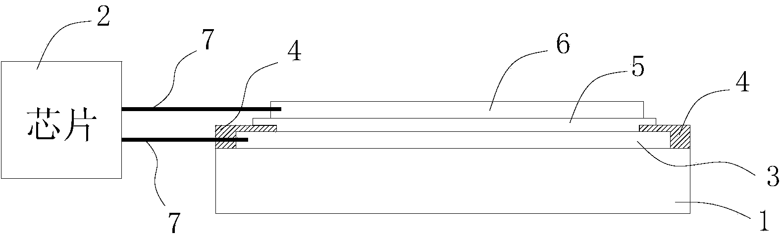
[0026] The invention discloses a monolithic glass capacitive touch screen structure, such as figure 1 As shown, it includes a glass substrate 1 and a chip 2, the first ITO film layer 3 is provided on the glass substrate 1, the edge of the first ITO film layer 3 is covered with ink 4, and the ink 4 needs to be applied during processing. Silk screen printing on the edge of the first ITO film layer 3, so that the ink 4 forms a frame, thereby effectively protecting the first ITO film layer 3, the first ITO film layer 3 is provided with an insulating transparent layer 5, and on the insulating transparent layer 5 A second ITO film layer 6 is provided. The first ITO film layer 3 and the second ITO film layer 6 are respectively etched with ITO traces, and the ITO traces are electrically connected to the chip 2 through a flexible circuit board 7 .

[002...


PUM


Abstract

The invention discloses a monolithic glass capacitive touch screen structure which comprises a glass substrate and a chip. The glass substrate is provided with a first ITO (indium-tin oxide) film, ink covers the edge of the first ITO film, the first ITO film is covered with an insulation transparent layer, the insulation transparent layer is covered with a second ITO film, and ITO wires are etched on the first ITO film and the second ITO film and are electrically connected with the chip via flexible circuit boards. The monolithic glass capacitive touch screen structure can meet the requirements of large size, low cost, high transmittance, thinness and light weight and the like.

Description

technical field [0001] The invention relates to a capacitive touch screen, in particular to a single glass capacitive touch screen structure and a processing method thereof. Background technique [0002] With the advancement of multimedia information technology and touch technology, capacitive touch screens have been widely used. Most of the existing capacitive touch screens adopt G+G structure, G+F structure, G+P structure and OGS structure, among which: [0003] The G+G structure is a double-layer glass structure of tempered glass + sensor glass. Due to the use of double-layer glass in this structure, the weight of the product is heavier and the thickness is thicker. higher; [0004] The G+F structure is a structure of tempered glass + FILM film. Due to the low light transmittance of the FILM material, it affects the light transmittance of the touch screen, resulting in poor imaging effect, and requires the use of bonding technology during processing, which has a high Pr...

Claims


Application Information

Patent Timeline
Patent Type & Authority Applications(China)
IPC IPC(8): G06F3/044
Inventor 马金成詹达勇光宣标童建超唐鑫
Owner SHENZHEN SANXIN JMT GLASS
Why Eureka
Try Eureka