Semiconductor device manufacturing method and stack type chip manufacturing method
A semiconductor and device technology, applied in the field of semiconductor preparation, can solve the problems of high cost, complex preparation process, low production capacity, etc., and achieve the effect of increasing production capacity, simplifying preparation process and reducing cost
- Summary
- Abstract
- Description
- Claims
- Application Information
AI Technical Summary
Problems solved by technology
Method used
Image

Examples
preparation example Construction
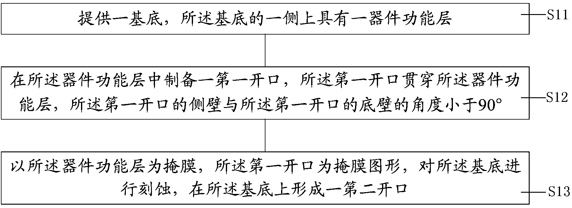
[0047]The core idea of the present invention is to provide a semiconductor device preparation method, comprising the following steps:
[0048] Step S11: providing a substrate with a device functional layer on one side of the substrate;
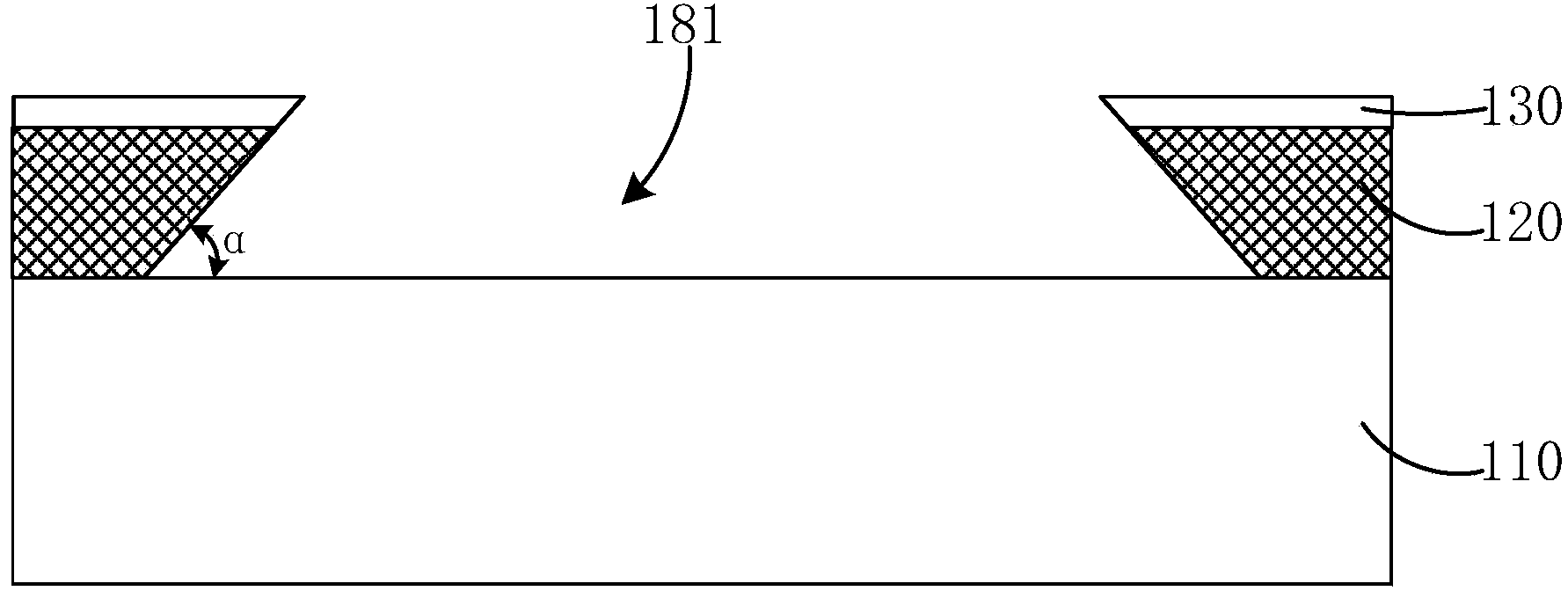
[0049] Step S12: Prepare a first opening in the device functional layer, the first opening runs through the device functional layer, and the angle between the side wall of the first opening and the bottom wall of the first opening is less than 90° °;
[0050] Step S13: Using the device functional layer as a mask and the first opening as a mask pattern, etching the substrate to form a second opening on the substrate.
[0051] The included angle between the side wall of the first opening and the bottom wall of the first opening is less than 90°, so that the top dimension of the first opening is smaller than the bottom dimension of the first opening, and the formed on the substrate When the second opening is described, the first opening is us...
no. 1 example
[0058] The following combination Figure 1-Figure 5 The semiconductor manufacturing method in this example will be described. in, figure 1 is a flow chart of the semiconductor manufacturing method according to the first embodiment of the present invention; Figure 2-Figure 5 It is a structural schematic diagram during the preparation process of the semiconductor preparation method according to the first embodiment of the present invention.
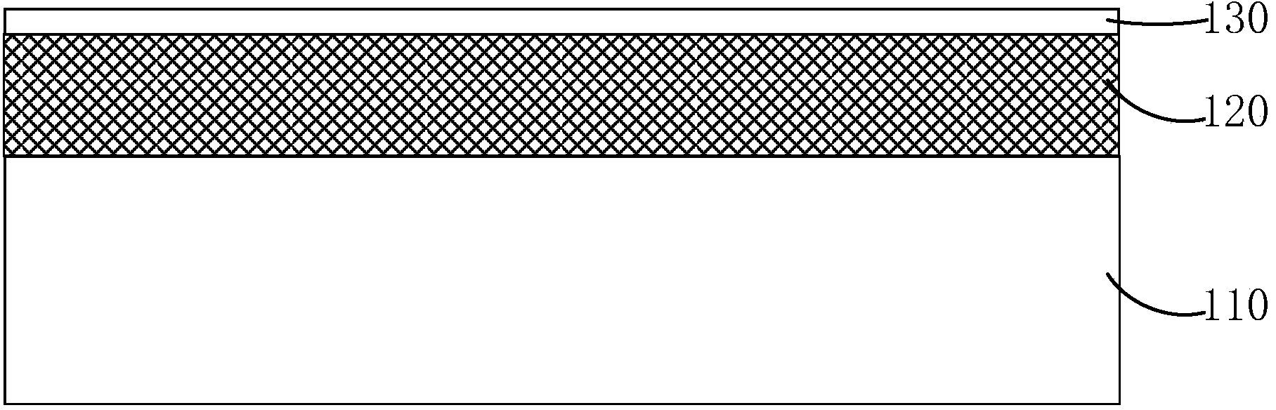
[0059] In the semiconductor manufacturing method of this embodiment, first, step S11 is performed to provide a substrate 110, and a device function layer 120 is provided on one side of the substrate 110, such as figure 2 shown. Among them, in figure 2 In the above, the materials of the substrate 110 and the device functional layer 120 are different. In other embodiments of the present invention, the materials of the substrate 110 and the device functional layer 120 may be the same, or may be the same layer.
[0060] Preferably, befo...
no. 2 example
[0065] see Figure 6-Figure 13 A method of manufacturing the stacked chip in this example will be described. in, Figure 6 is a flow chart of the method for preparing stacked chips according to the second embodiment of the present invention; Figure 7-Figure 13 It is a structural schematic diagram during the preparation process of the method for preparing stacked chips according to the second embodiment of the present invention. The method for preparing the stacked chip of the second embodiment uses the method of the first embodiment to prepare the second opening, and the specific steps are as follows:
[0066] First, proceed to step S21, providing a first chip 200 and a second chip 300, such as Figure 7 As shown, the first chip 200 includes a first substrate 210 and a first epitaxial layer 220 located on one side of the first substrate 210 , and the first epitaxial layer 220 includes a first interconnection structure 221 . The second chip 300 includes a second substrate ...
PUM
 Abstract
Description
Claims
Application Information
 - R&D Engineer
- R&D Manager
- IP Professional
- Industry Leading Data Capabilities
- Powerful AI technology
- Patent DNA Extraction
Browse by: Latest US Patents, China's latest patents, Technical Efficacy Thesaurus, Application Domain, Technology Topic.
© 2024 PatSnap. All rights reserved.Legal|Privacy policy|Modern Slavery Act Transparency Statement|Sitemap