A test structure for array substrate and its manufacturing method

A technology for testing structures and array substrates, used in instruments, semiconductor devices, circuits, etc., can solve problems such as accumulation of static electricity, large static electricity, and static damage to test structures, to eliminate static electricity accumulation, increase complexity, and prevent electrostatic damage. Effect

Active Publication Date: 2018-07-10
SHANGHAI AVIC OPTOELECTRONICS +1
View PDF5 Cites 0 Cited by
  • Summary
  • Abstract
  • Description
  • Claims
  • Application Information

AI Technical Summary

Problems solved by technology

[0006] Using this method to test the components under test on the array substrate, the process is simple and the test effect is good, but this method has disadvantages. During the manufacturing process of the test structure, a large static electricity is often generated, and the test structure is usually formed on glass. On the substrate, these static electricity can accumulate on the glass, causing electrostatic damage to the test structure
In particular, the gate test line 1 is a large area of ​​metal, and the source and drain electrodes of the thin film transistor are also composed of metal, which will accumulate static electricity. Before the pixel electrode is made, it is often at the edge where the source drain and the gate test line 5 Electrostatic damage occurs, which causes poor panel display

Method used


Image

  • A test structure for array substrate and its manufacturing method
  • A test structure for array substrate and its manufacturing method
  • A test structure for array substrate and its manufacturing method

Examples


specific Embodiment approach 1

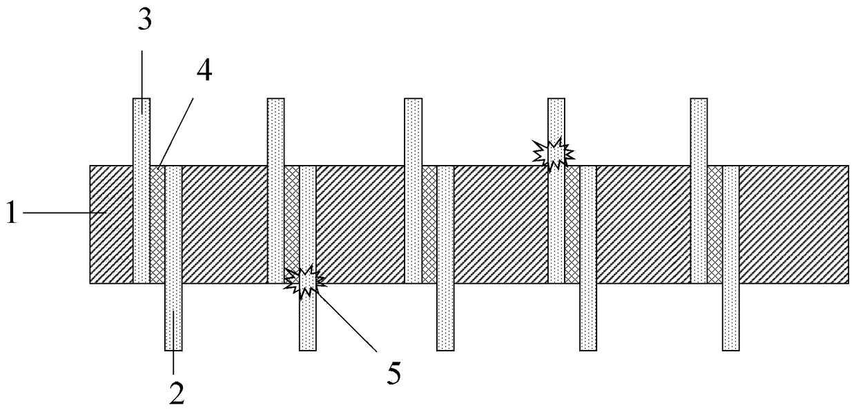
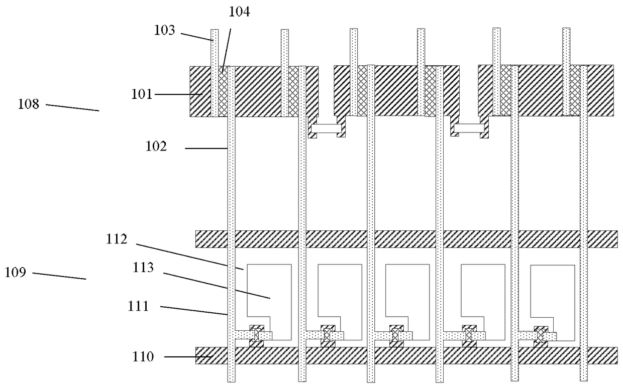
[0045] figure 2 is a top view of the array substrate in this embodiment, as shown in figure 2As shown, the array substrate includes a peripheral area 108 and a display area 109 . In the peripheral area 108, there is a gate test line 101, on which there are source 103, channel layer 104, and drain 102 of the thin film transistor, and the gate of the thin film transistor is a part of the gate test line , the cross-sectional view of the thin film transistor is shown in Figure 7 As shown, there is a gate insulating film 105 on the gate test line 101, a channel layer 104 on the gate insulating film 105, and a source electrode 103 and a drain electrode 102 covering part of the channel layer on the channel layer 104, Finally, there is a protection layer 106 on the source and drain electrodes.

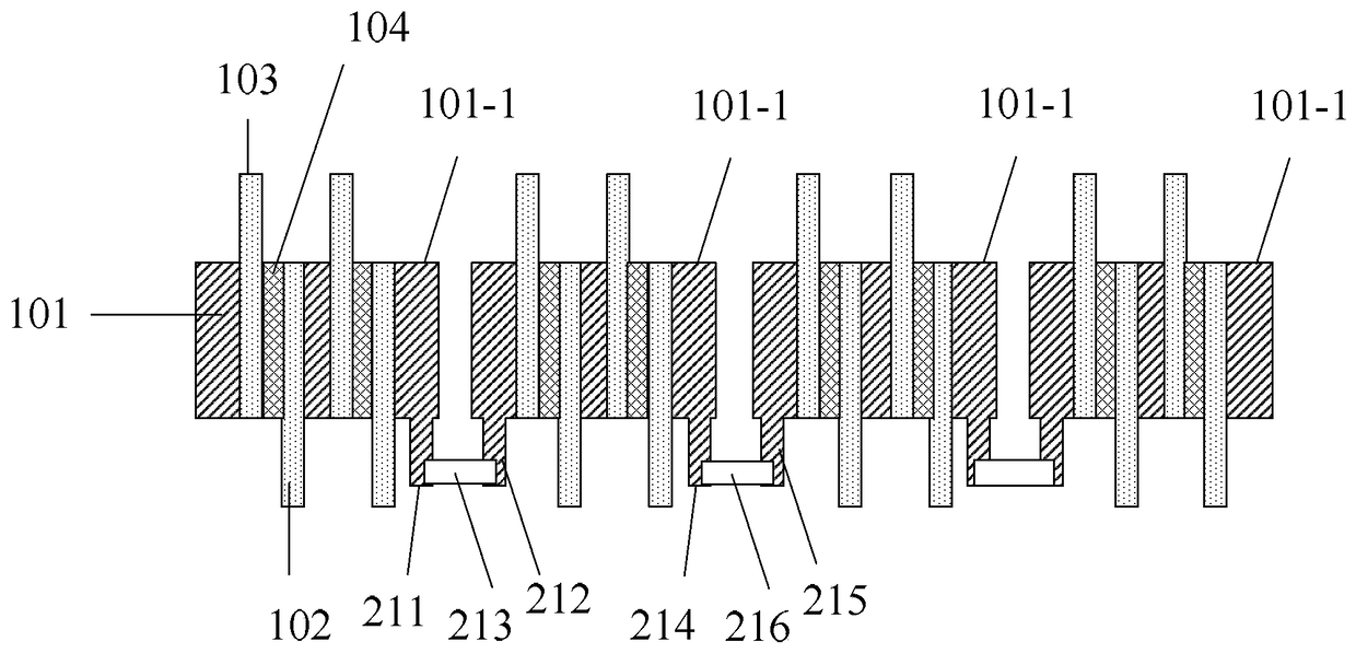
[0046] A more detailed partial diagram of the gate test line is shown in image 3 As shown, the gate test line 101 is composed of a plurality of gate test line segments 101-1 separated ...


PUM


Abstract

The invention discloses a test structure and a manufacturing method thereof. The test structure includes a thin film transistor, which is arranged in the peripheral area of ​​the array substrate; data lines are arranged in the display area of ​​the array substrate, and the thin film transistor has a The source electrode or the drain electrode is electrically connected to the data line in the display area; the gate test line is used as the gate of the thin film transistor and includes a plurality of gate test line segments separated from each other; the gate test line segment passes through The conductive lines are electrically connected together. The test structure can eliminate the accumulation of static electricity in the gate test line, prevent electrostatic damage between the gate test line and the data line, and does not increase the complexity of the process.

Description

technical field [0001] The invention relates to the technical field of liquid crystal display, in particular to a test structure for an array substrate and a manufacturing method thereof. Background technique [0002] At present, liquid crystal displays have gradually become the mainstream of display equipment development due to their advantages of high definition, true color video display, light and thin appearance, low power consumption, and no radiation. A liquid crystal display generally includes a liquid crystal display panel for displaying pictures and a circuit part for supplying signals to the liquid crystal display panel. The liquid crystal display panel usually includes a color filter substrate and an array substrate, which are bonded to each other by a frame glue and separated by a gap, and liquid crystal material is injected into the gap between the color filter substrate and the array substrate. [0003] The array substrate is a layered structure formed by sett...

Claims


Application Information

Patent Timeline
Patent Type & Authority Patents(China)
IPC IPC(8): G02F1/1362G02F1/1368G02F1/13H01L23/544
Inventor 梁艳峰
Owner SHANGHAI AVIC OPTOELECTRONICS
Why Eureka
Try Eureka