Forming method of multiple patterns

A technology of multiple graphics and graphics, which is applied in the fields of electrical components, semiconductor/solid-state device manufacturing, circuits, etc., can solve the problems of high cost and complicated process of forming multiple graphics

Inactive Publication Date: 2014-07-16
SEMICON MFG INT (SHANGHAI) CORP
View PDF4 Cites 10 Cited by
  • Summary
  • Abstract
  • Description
  • Claims
  • Application Information

AI Technical Summary

Problems solved by technology

[0009] The problem to be solved by the present invention is that the forming method of multiple patterns in the prior art is complex in process and high in cost

Method used


Image

  • Forming method of multiple patterns
  • Forming method of multiple patterns
  • Forming method of multiple patterns

Examples


Embodiment Construction

[0031] It can be seen from the background art that the prior art method for forming multiple patterns is complicated in process and high in cost.

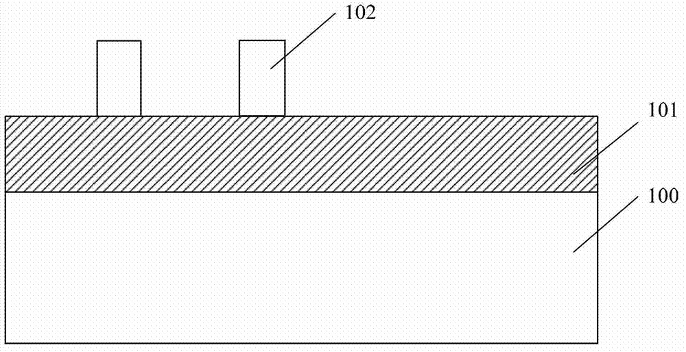
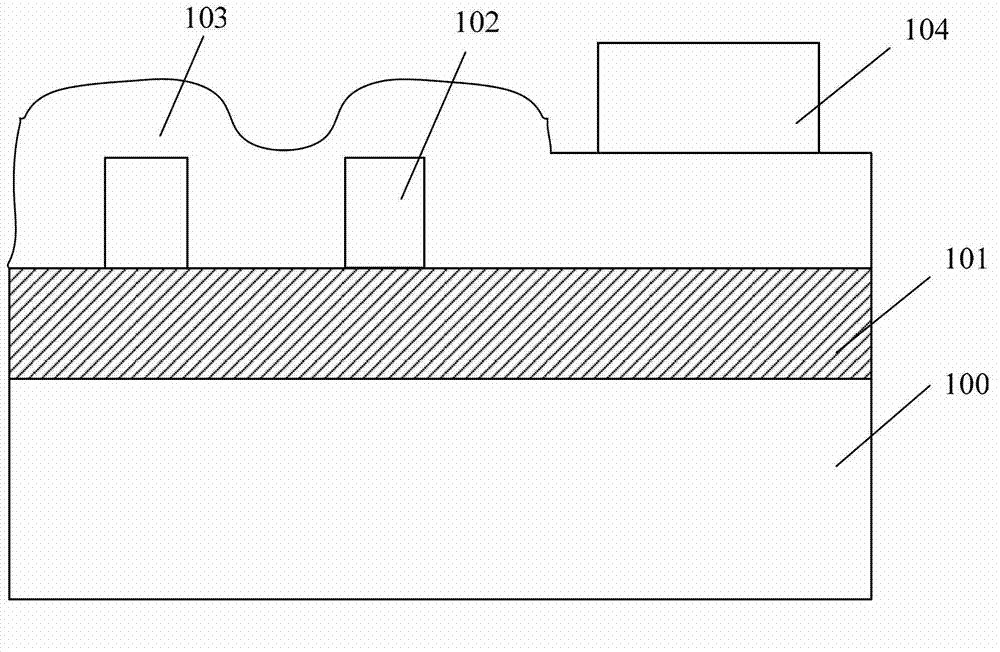
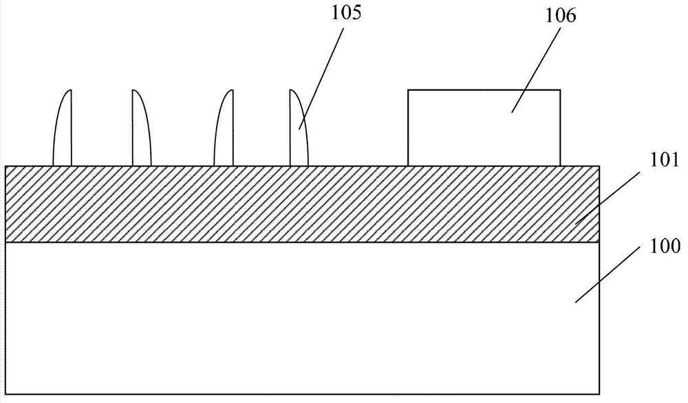
[0032] The inventors of the present invention have studied the formation method of multiple patterns in the prior art, and found that the etching mask of the small-scale pattern in the prior art is formed by sidewalls around the etching sacrificial layer, while the etching mask of the large-scale pattern is formed by Formed by photolithography and etching process. Since the etching sacrificial layer needs to be removed later to form separate sidewalls, the etching sacrificial layer and the etching mask layer of the large-scale pattern cannot be formed at the same time, and different photolithography processes are required to form, resulting in The process is complex and requires multiple photolithography.

[0033] Based on the above studies, the inventors of the present invention have proposed a method for forming multiple pattern...


PUM


Abstract

Disclosed is a forming method of multiple patterns. The method comprises: providing a semiconductor substrate, and forming an etching target layer on the semiconductor substrate; forming a first mask layer on the etching target layer, the first mask layer being provided with a first dimension pattern and a second dimension pattern; forming a first side wall material layer and a second side wall material layer on the etching target layer; performing back-etching on the second side wall material layer to form a side wall, and by taking the side wall as a mask, etching the first side wall material layer, the side wall disposed around the first dimension pattern and the residual first side wall material layer forming a third dimension pattern, the side wall disposed around the second side wall material layer and the residual first side wall material layer forming a fourth dimension pattern; and by taking the first dimension pattern, the second dimension pattern, the third dimension pattern and the fourth dimension pattern as masks, etching the etching target layer, and forming a target pattern. The forming method of the multiple patterns has the advantages of simple process and low cost.

Description

technical field [0001] The invention relates to the technical field of semiconductors, in particular to a method for forming multiple patterns. Background technique [0002] With the continuous shrinking of the minimum line width and spacing of integrated circuit design, when the feature size of the exposure line is close to the theoretical resolution limit of the exposure system, the lithographic imaging will be severely distorted, resulting in a serious decline in the quality of the lithographic pattern. . In order to reduce the impact of the optical proximity effect, the industry has proposed a lithography resolution enhancement technology, in which the double patterning technology (DPT: Double Patterning Technology) is considered to fill the gap between immersion lithography and extreme ultraviolet lithography (EUV) A strong guarantee for the gap. Double patterning technology usually forms an etching sacrificial layer on the material layer to be etched, and forms sidew...

Claims


Application Information

Patent Timeline
Patent Type & Authority Applications(China)
IPC IPC(8): H01L21/027H01L21/3065
CPCH01L21/0337H01L21/0338H01L21/32139
Inventor 洪中山
Owner SEMICON MFG INT (SHANGHAI) CORP
Why Eureka
Try Eureka