
Organic light-emitting display device and manufacturing method thereof

A technology of light-emitting display and manufacturing method, which is applied in the manufacturing of semiconductor/solid-state devices, semiconductor devices, electrical components, etc., can solve the problems of scratches, touches, low yield of OLED displays, and many defective products, etc., to improve the yield Effect

Active Publication Date: 2014-07-16
WUHAN TIANMA MICRO ELECTRONICS CO LTD +1
View PDF7 Cites 14 Cited by
  • Summary
  • Abstract
  • Description
  • Claims
  • Application Information

AI Technical Summary

Problems solved by technology

However, in the structure of the above-mentioned OLED display, when the OLED display panel 01 and the touch panel 02 are assembled, it is easy to scratch, touch, etc. on the contact interface between the OLED display panel 01 and the touch panel 02, so More defective products are produced, resulting in a lower yield rate of OLED displays in the prior art

Method used


Image

  • Organic light-emitting display device and manufacturing method thereof
  • Organic light-emitting display device and manufacturing method thereof
  • Organic light-emitting display device and manufacturing method thereof

Examples


Embodiment Construction

[0031] As mentioned in the background section, the yield rate of OLED displays in the prior art is low.

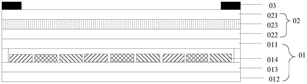
[0032] Moreover, in the OLED display in the prior art, the OLED display panel includes: an upper substrate and a lower substrate, a TFT wiring layer located on the lower substrate facing the surface of the upper substrate, and a TFT wiring layer located on the surface of the TFT wiring layer. Organic light-emitting layer; the touch panel includes: an upper substrate and a lower substrate, and a touch electrode layer located between the upper substrate and the lower substrate, so that after the OLED display panel and the touch panel are assembled together, As a result, the thickness of the OLED display in the prior art is relatively large.

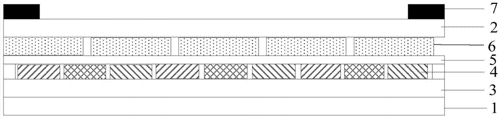
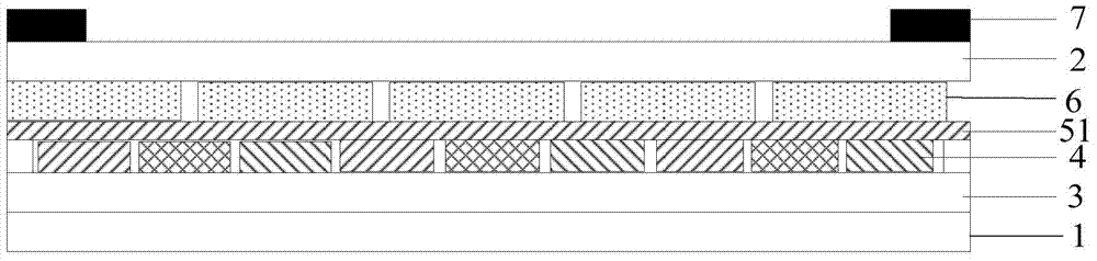
[0033] In view of this, an embodiment of the present invention provides an organic light emitting display device, including:

[0034] a first substrate and a second substrate oppositely arranged;

[0035] a TFT wiring layer disposed o...


PUM


Abstract

The embodiment of the invention discloses an organic light-emitting display device and a manufacturing method thereof. The device comprises a first substrate, a second substrate, a TFT wiring layer, an organic light-emitting layer, a first insulation layer and a touch electrode layer, wherein the first substrate and the second substrate are arranged oppositely; the TFT wiring layer is arranged on the side, facing the second substrate, of the first substrate; the organic light-emitting layer is arranged on the surface of the TFT wiring layer; the first insulation layer is arranged on the surface of the organic light-emitting layer; the touch electrode layer is arranged on the surface of the first insulation layer. Thus, in the organic light-emitting display device, the touch electrode layer is arranged between the first substrate and the second substrate, the organic light-emitting layer and the touch electrode layer are insulated with each other through the first insulation layer, and therefore the technology that an OLED display panel is assembled with a touch panel in the prior art is avoided; accordingly, the problem that defective products are generated due to scratching, touching and the like in the assembly process of the OLED display panel and the touch panel is solved, and the yield of organic light-emitting display devices is increased.

Description

technical field [0001] The present invention relates to the technical field of light-emitting display, in particular to an organic light-emitting display device and a manufacturing method thereof. Background technique [0002] At present, there are many TP (touch electrode layer) compatible methods for OLED (Organic Light-Emitting Diode, organic light-emitting diode) displays, and most of them are made separately from TP and OLED and then assembled. Such as figure 1 As shown, the OLED display in the prior art includes: an OLED display panel 01 , a touch panel 02 located on the surface of the OLED display panel 01 , and a cover plate 03 located on the surface of the touch panel 02 . However, in the structure of the above-mentioned OLED display, when the OLED display panel 01 and the touch panel 02 are assembled, it is easy to scratch, touch, etc. on the contact interface between the OLED display panel 01 and the touch panel 02, so More defective products are produced, resul...

Claims


Application Information

Patent Timeline
IPC IPC(8): H01L27/32H01L51/56
Inventor 熊志勇顾寒昱钱栋
Owner WUHAN TIANMA MICRO ELECTRONICS CO LTD
Features
  • Generate Ideas
  • Intellectual Property
  • Life Sciences
  • Materials
  • Tech Scout
  • Unparalleled Data Quality
  • Higher Quality Content
  • 60% Fewer Hallucinations
Learn More