Embedded germanium-silicon epitaxy dislocation fault improving method

An embedded germanium-silicon, dislocation technology, applied in electrical components, semiconductor/solid-state device manufacturing, circuits, etc., can solve problems such as interface defects

Inactive Publication Date: 2014-07-23
SHANGHAI HUALI MICROELECTRONICS CORP
View PDF4 Cites 4 Cited by
  • Summary
  • Abstract
  • Description
  • Claims
  • Application Information

AI Technical Summary

Problems solved by technology

[0007] The present invention is aimed at the conventional PMOS device in the prior art, which inevitably has certain defects on the trench surface after cleaning, resulting in defect sources at the interface after epitaxial growth, and serious defects may continue to the growth surface of silicon germanium, etc. Provide a method for improving dislocation defects in embedded germanium silicon epitaxy

Method used


Image

  • Embedded germanium-silicon epitaxy dislocation fault improving method
  • Embedded germanium-silicon epitaxy dislocation fault improving method
  • Embedded germanium-silicon epitaxy dislocation fault improving method

Examples


Embodiment Construction

[0018] In order to illustrate the technical content, structural features, achieved goals and effects of the present invention in detail, the following will be described in detail in conjunction with the embodiments and accompanying drawings.

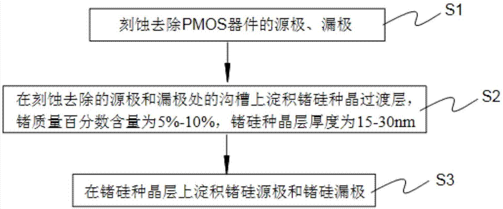
[0019] see figure 1 , figure 1 Shown is a flow chart of the method for improving dislocation defects in embedded silicon germanium epitaxy according to the present invention. The method for improving the embedded silicon germanium epitaxial dislocation defect comprises the following steps,

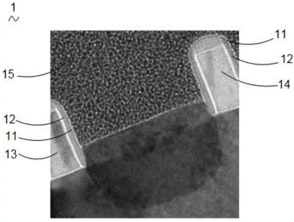
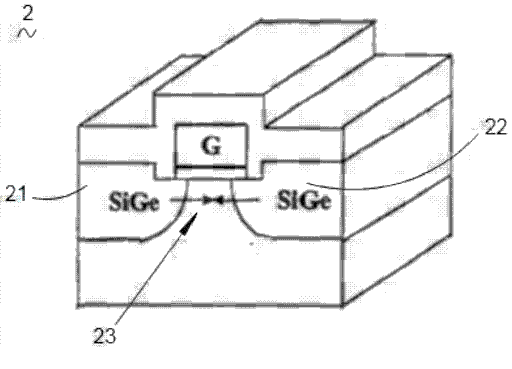
[0020] Executing step S1: removing the first source and the first drain of the first PMOS device 1 by etching;

[0021] Executing step S2: depositing a germanium-silicon seed crystal transition layer 12 on the groove 11 at the first source and the first drain removed by etching, and the germanium-silicon seed transition layer 12 has a quality of germanium The percentage content is 5% to 10%, and the film thickness of the silicon germanium seed t...


PUM

PropertyMeasurementUnit
Film thicknessaaaaaaaaaa

Abstract

The invention discloses an embedded germanium-silicon epitaxy dislocation fault improving method. The method includes the following steps that firstly, the source and drain of a PMOS device are removed in an etching mode; secondly, a germanium-silicon seed crystal transition layer is arranged on a groove where the source and the drain are removed in the etching mode in a deposition mode, wherein the mass percent of germanium in the germanium-silicon seed crystal transition layer ranges from 5% to 10%, and the film layer thickness of the germanium-silicon seed crystal transition layer ranges from 15 nm to 30 nm; thirdly, a germanium-silicon source and a germanium-silicon drain are arranged on the germanium-silicon seed crystal transition layer in a deposition mode. Boundary surfaces between the germanium-silicon source and germanium-silicon drain of the PMOS device prepared through the embedded germanium-silicon epitaxy dislocation fault improving method and a substrate are clear and smooth, dislocation faults are greatly improved, and stress relaxation is alleviated.

Description

technical field [0001] The invention relates to the technical field of semiconductors, in particular to a method for improving embedded silicon germanium epitaxial dislocation defects. Background technique [0002] As we all know, the performance of CMOS circuits is largely limited by that of PMOS. Therefore, any technology that can improve the performance of PMOS to the level of NMOS is considered to be beneficial. see image 3 , image 3 The schematic diagram of the PMOS structure of the SiGe source / drain implantation straining technology is shown. In the second PMOS device 2 of 90nm, the researchers of Intel etched and removed the source and drain of the device, and then redeposited the silicon germanium layer, so that the second source 21 and the second drain 22 would be opposite to all The second channel 23 generates a compressive stress, thereby improving the transmission characteristics of the second PMOS device 2 . [0003] As known to those skilled in the art, th...

Claims


Application Information

Patent Timeline
IPC IPC(8): H01L21/336
CPCH01L21/823814
Inventor 周海锋谭俊高剑琴李润领
Owner SHANGHAI HUALI MICROELECTRONICS CORP
Why Eureka
Try Eureka