Preparation method for backgate thin film transistor storage

A thin-film transistor and memory technology, applied in semiconductor/solid-state device manufacturing, electrical components, circuits, etc., can solve the problems of thin film compactness and lack of uniformity of large-area components, and achieve improved large-area uniformity and easy integration. , the effect of clear interface

Inactive Publication Date: 2012-07-18
FUDAN UNIV
View PDF4 Cites 14 Cited by
  • Summary
  • Abstract
  • Description
  • Claims
  • Application Information

AI Technical Summary

Problems solved by technology

However, the current preparation technology of the a-IGZO channel layer of TFT memory is based on traditional physical vapor deposition (PVD), such as radio frequency magnetron sputtering and pulsed laser deposition, etc., and the films deposited by these methods are dense There are deficiencies in the homogeneity of the properties and large-area components

Method used


Image

  • Preparation method for backgate thin film transistor storage
  • Preparation method for backgate thin film transistor storage
  • Preparation method for backgate thin film transistor storage

Examples


Embodiment Construction

[0031] The invention will be described in detail below in conjunction with the accompanying drawings and specific examples.

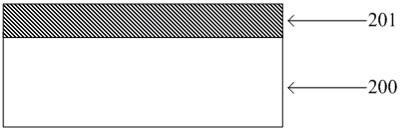
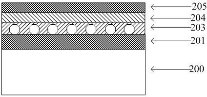
[0032] Step 1: Select a heavily doped P-type single crystal silicon wafer with a resistivity of 0.008-0.100 Ω cm as the substrate, and clean the silicon wafer through a standard RCA cleaning process, and then remove the surface of the silicon wafer with hydrofluoric acid oxide layer. refer to figure 1 , the cleaned silicon wafer is shown as 200 in the figure.

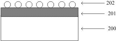
[0033] Step 2: On the cleaned silicon wafer, use ALD method to deposit and grow Al 2 o 3 film, such as figure 1 Shown on the 201st floor. al 2 o 3 The thickness of the film is 15-200nm; during the deposition process, the substrate temperature is controlled at 100-300 oC between; growing Al 2 o 3 The reaction sources are trimethylaluminum and water vapor.

[0034] Step 3: Using ALD method on Al 2 o 3 Deposit a layer of Ru nanocrystals on the film, such as figure 2 Shown in 202. ...


PUM


Abstract

The invention belongs to the technical field of semiconductor integrated circuits and particularly discloses a preparation method for a backgate thin film transistor storage. The method mainly comprises the following steps of: using a heavily doped P type monocrystalline silicon piece as a substrate and an extraction electrode of a gate; growing an Al2O3 thin film by an atomic layer deposition (ALD) method, and using the Al2O3 thin film as a charge baffling layer; depositing a metal nano crystal by the ALD method, and using the metal nano crystal as a charge capturing layer; depositing a SiO2/HfO2/Al2O3 laminated structure by the ALD method, and using the laminated structure as a tunneling layer of the storage; depositing an IGZO thin film by the ALD method, forming a source area by a photoetching and wet-method etching process, and using the source area as a conducting channel; and forming source and drain areas by photoetching technology, depositing a layer of metal, and processing a source electrode and a drain electrode by lift-off technology. The electrical properties of the channel can be well adjusted and controlled by the method, the large-area uniformity of the performance of the storage can be improved, and the reliability such as data preservation property and the tolerance of the storage can be improved.

Description

technical field [0001] The invention belongs to the technical field of semiconductor integrated circuits, and in particular relates to a method for preparing a back gate thin film transistor memory. Background technique [0002] With the maturity and development of thin-film transistor (TFT) process technology, non-volatile TFT memory is becoming a research hotspot for researchers at home and abroad. At present, most TFT memories use polysilicon as the conductive channel. However, since there are a large number of grain boundaries in the polysilicon channel, the traps located at the grain boundaries will trap part of the induced inversion charges, which will cause the turn-on voltage of the memory to shift. In addition, the TFT memory based on the polysilicon channel will show serious threshold voltage fluctuation after being subjected to the bias stress of the drain and the gate, thereby affecting the reliability of the device [1]. It can be seen that polysilicon is not a...

Claims


Application Information

Patent Timeline
Patent Type & Authority Applications(China)
IPC IPC(8): H01L21/8256H01L21/443
Inventor 丁士进崔兴美陈笋王鹏飞张卫
Owner FUDAN UNIV
Why Eureka
Try Eureka