Light-emitting diode and laser of p-GaN/ZnO-based multi-quantum well/n-ZnO structure and preparation method

A light-emitting diode, p-gan technology, applied in lasers, phonon exciters, laser parts and other directions, to achieve the effect of improving emission efficiency, stable and reliable p-type conductivity, and high crystal quality

Inactive Publication Date: 2016-07-13
ZHEJIANG UNIV
View PDF7 Cites 0 Cited by
  • Summary
  • Abstract
  • Description
  • Claims
  • Application Information

AI Technical Summary

Problems solved by technology

At present, in the field of ZnO-based light-emitting diodes and lasers, there is no report on p-GaN / ZnO / ZnMgO multi-quantum well / n-ZnO structure at home and abroad

Method used


Image

  • Light-emitting diode and laser of p-GaN/ZnO-based multi-quantum well/n-ZnO structure and preparation method

Examples


Embodiment 1

[0032] 1) Substrate cleaning: Put the sapphire substrate with the p-GaN layer into acetone, alcohol and deionized water in order to ultrasonically clean it for 10 min, rinse with deionized water, and blow dry with nitrogen.

[0033] 2) Substrate pretreatment: put the above-mentioned cleaned substrate into the molecular beam epitaxy system pretreatment chamber and bake for 3 hours at a temperature of 300°C; then put it into a high-vacuum growth chamber for high temperature treatment at 800°C for 30 minutes.

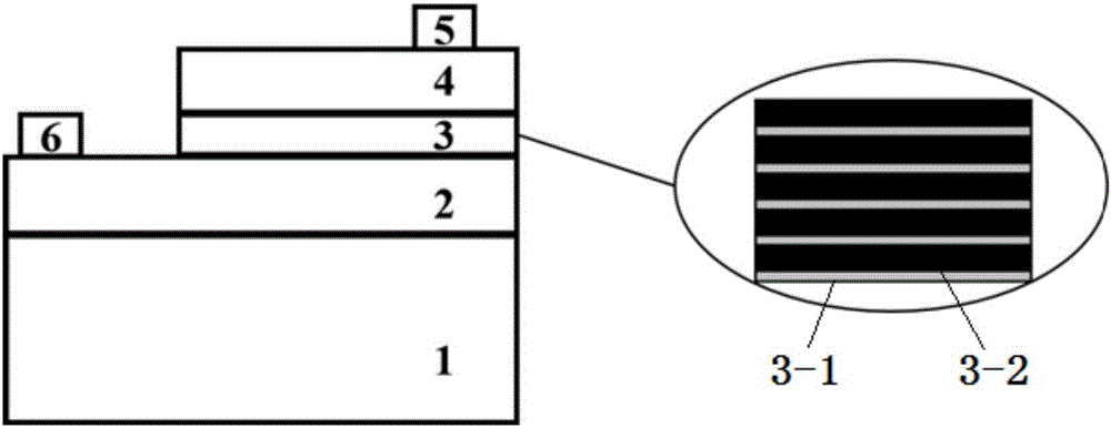
[0034] 3) Deposit 5 cycles of ZnO / ZnMgO multiquantum wells on the p-GaN layer by molecular beam epitaxy, and reserve the area for growing the first electrode at the same time, using pure metal Zn (purity 99.9998%) as the Zn source, pure metal Mg (99.9999% pure) as the source of Mg, pure O activated by RF 2 (purity is 99.9999%) is the O source, the substrate temperature is 650 ° C, the Zn source furnace temperature is 250 ° C, the Mg source furnace temperature is 350 ° C, t...

Embodiment 2

[0038] 1) Substrate cleaning: Put the sapphire substrate with the p-GaN layer into acetone, alcohol and deionized water in order to ultrasonically clean it for 10 min, rinse with deionized water, and blow dry with nitrogen.

[0039] 2) Substrate pretreatment: put the above-mentioned cleaned substrate into the molecular beam epitaxy system pretreatment chamber and bake for 3 hours at a temperature of 300°C; then put it into a high-vacuum growth chamber for high temperature treatment at 800°C for 30 minutes.

[0040] 3) Deposit 5 cycles of ZnO / ZnMgO multiquantum wells on the p-GaN layer by molecular beam epitaxy, and reserve the area for growing the first electrode at the same time, using pure metal Zn (purity 99.9998%) as the Zn source, pure metal Mg (99.9999% pure) as the source of Mg, pure O activated by RF 2 (purity is 99.9999%) is the O source, the substrate temperature is 700°C, the Zn source furnace temperature is 250°C, the Mg source furnace temperature is 355°C, the oxy...

Embodiment 3

[0044] 1) Substrate cleaning: Put the sapphire substrate with the p-GaN layer into acetone, alcohol and deionized water in order to ultrasonically clean it for 10 min, rinse with deionized water, and blow dry with nitrogen.

[0045] 2) Substrate pretreatment: put the above-mentioned cleaned substrate into the molecular beam epitaxy system pretreatment chamber and bake for 3 hours at a temperature of 300°C; then put it into a high-vacuum growth chamber for high temperature treatment at 800°C for 30 minutes.

[0046] 3) Using molecular beam epitaxy to deposit 8 cycles of ZnO / ZnMgO multiquantum wells on the p-GaN layer, while reserving the area for growing the first electrode, using pure metal Zn (purity 99.9998%) as the Zn source, pure metal Mg (99.9999% pure) as the source of Mg, pure O activated by RF 2 (purity is 99.9999%) is the O source, the substrate temperature is 700 ° C, the Zn source furnace temperature is 250 ° C, the Mg source furnace temperature is 360 ° C, the oxyg...


PUM

PropertyMeasurementUnit
thicknessaaaaaaaaaa
thicknessaaaaaaaaaa
thicknessaaaaaaaaaa

Abstract

The invention discloses a light-emitting diode and laser of a p-GaN/ZnO-based multi-quantum well/n-ZnO structure and a preparation method. The light-emitting diode and laser includes a p-GaN layer, a ZnO-ZnMgO multi-quantum well layer, an n-ZnO layer and metal electrodes. The preparation method includes the steps of: first adopting a molecular beam epitaxy method to successively prepare the ZnO/ZnMgO multi-quantum well layer and the n-ZnO layer on a p-GaN film; and then plating the metal electrodes in p-GaN and n-ZnO regions respectively. The device prepared by the invention adopts the ZnO/ZnMgO multi-quantum well as an active layer, and a threshold value of the light-emitting diode and laser be lowered and luminous efficiency can be improved; in addition, to solve the problem that efficient and stable p-ZnO is difficult to realize in a homogeneous structure, the device adopts p-GaN as a hole injection layer; and at the same time, compared with other p type materials, GaN has the advantages of having the same structure as ZnO and having low epitaxial mismatch.

Description

technical field [0001] The invention relates to a preparation method of a light-emitting diode and a laser, in particular to a light-emitting diode with a p-GaN / ZnO-based multi-quantum well / n-ZnO structure, a laser and a preparation method thereof, belonging to the field of semiconductor optoelectronic devices. Background technique [0002] In recent years, short-wavelength light-emitting diodes and lasers have become research hotspots in the field of semiconductor optoelectronics due to their advantages of high efficiency and energy saving. As a wide-bandgap semiconductor material, ZnO has a direct bandgap energy band structure, and the room temperature bandgap width is 3.37eV; in addition to the advantages of stable physical and chemical properties and abundant raw materials, the exciton binding energy of ZnO is as high as 60meV, which is much higher than that of GaN. (25meV), ZnSe (22meV) and other semiconductor materials are also higher than room temperature thermal ener...

Claims


Application Information

Patent Timeline
Patent Type & Authority Applications(China)
IPC IPC(8): H01L33/06H01L33/14H01L33/00H01S5/347
CPCH01L33/06H01L33/0087H01L33/14H01S5/347H01S2301/173H01S2304/02
Inventor 叶志镇陈珊珊潘新花黄靖云何海平吕斌
Owner ZHEJIANG UNIV
Why Eureka
Try Eureka