

Preparation method for water solution thin film transistor
A thin-film transistor and aqueous solution technology, applied in the manufacture of semiconductor/solid-state devices, nanotechnology for materials and surface science, semiconductor devices, etc., can solve problems such as unfavorable sustainability, green environmental protection, increased experiment costs, and damage to the natural environment , to achieve the effect of reducing the preparation cost, low cost, and avoiding high temperature impurity
- Summary
- Abstract
- Description
- Claims
- Application Information
AI Technical Summary
Problems solved by technology
Method used
Image

Examples
Embodiment
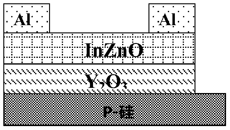
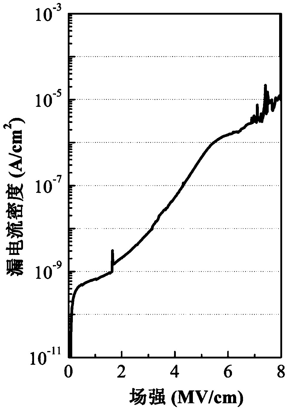
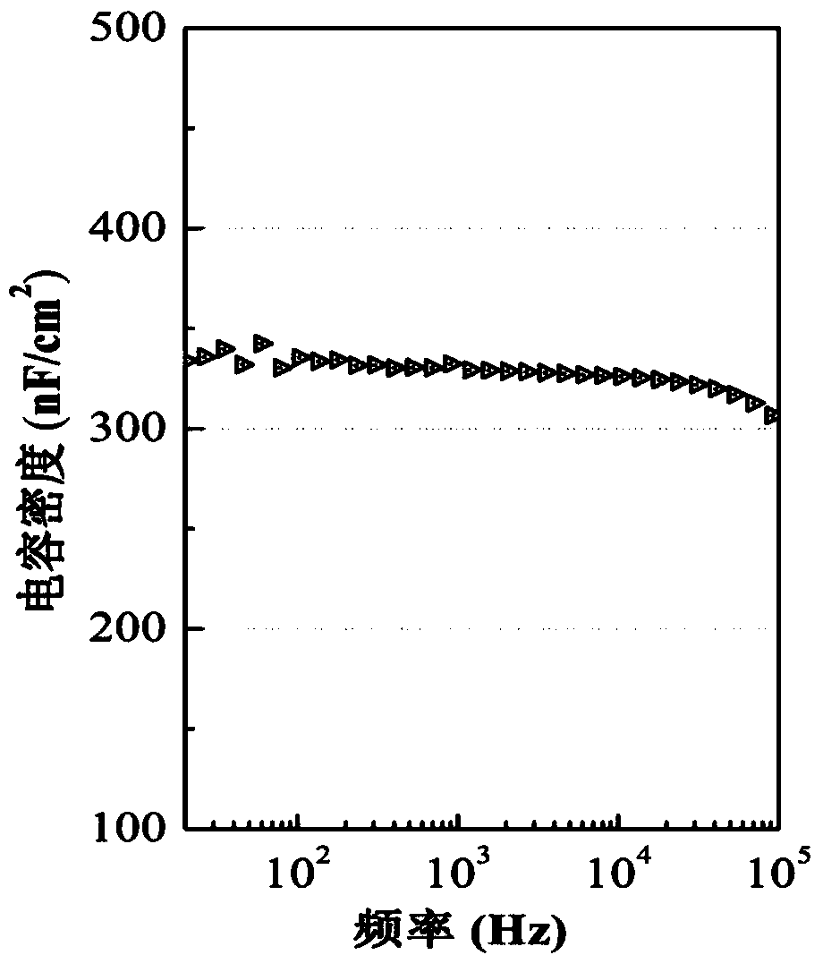
[0023] Yttrium nitrate, zinc nitrate and indium nitrate powders in this embodiment are all purchased from Aladdin Company, and the purity is greater than 98%; its bottom gate structure is based on ultra-thin yttrium oxide (Y 2 o 3 ) is a high-k dielectric layer and an indium zinc oxide (IZO) thin film is the preparation process based on an aqueous solution thin film transistor as a channel layer:
[0024] (1) Preparation of ultra-thin Y by spin coating with aqueous solution method 2 o 3 High-k dielectric films:
[0025] Step 1: Select commercially purchased single-sided polished low-resistance silicon as the substrate (ρ<0.0015Ω·cm) and the gate electrode, and the low-resistance silicon substrate is ultrasonically cleaned with hydrofluoric acid, acetone, and alcohol for 10 minutes each. After repeated washing with deionized water, blow dry with high-purity nitrogen;
[0026] Step 2: Dissolve yttrium nitrate at 0.2M in the mixed solution, weigh 10mL of deionized water, weig...
PUM
| Property | Measurement | Unit |
|---|---|---|
| Resistivity | aaaaa | aaaaa |
| Thickness | aaaaa | aaaaa |
Abstract
Description
Claims
Application Information