Semiconductor light emitting device preparation method based on laser stripping
A light-emitting device, laser lift-off technology, applied in semiconductor/solid-state device manufacturing, semiconductor devices, electrical components, etc., can solve problems such as GaN film cracking, and achieve the effect of improving yield and ensuring integrity
- Summary
- Abstract
- Description
- Claims
- Application Information
AI Technical Summary
Problems solved by technology
Method used
Image
Examples
preparation example Construction
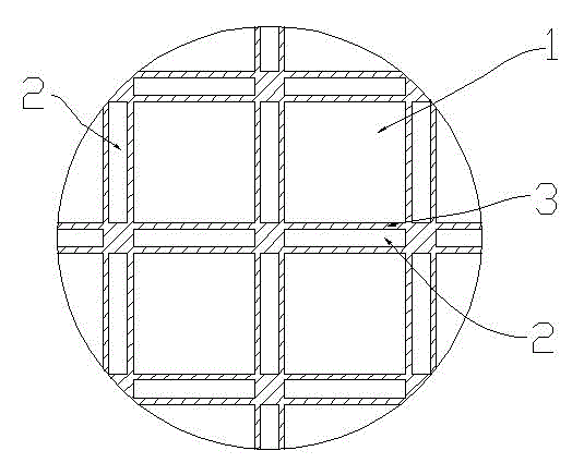
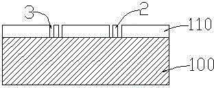
[0022] The present invention provides a method for preparing a semiconductor light emitting device, including the following steps: sequentially growing a buffer layer, an N-type GaN layer, an active layer, and a P-type GaN layer on a sapphire substrate 100 to form an epitaxial layer 110; and etching the epitaxial layer From layer 110 to the exposed sapphire substrate 100 to produce a plurality of discrete dies 1, a part of the epitaxial layer 110 is reserved between every two adjacent dies 1 as isolation tape 2, and the gap between different dies 1 The isolation tape 2 is discrete; the sapphire substrate 100 is removed by a laser lift-off method.
[0023] The structure of the etched epitaxial layer 110 is as figure 1 As shown, a part of the epitaxial layer is reserved as an isolation band 2 between every two adjacent dies 1, and the isolation band 2 is discontinuous, and the width of the isolation band 2 is 5-100 microns. A groove 3 is formed between the isolation band 2 and the ...
Embodiment 1
[0025] Such as Figure 2a As shown, a buffer layer, an N-type GaN layer, an active layer, and a P-type GaN layer are sequentially grown on the sapphire substrate 100 to form an epitaxial layer 110. The sapphire substrate 100 is mechanically ground, thinned, and polished. Such as Figure 2b As shown, the epitaxial layer 110 is dry-etched by ICP or RIE, and the epitaxial layer 110 is etched through to expose the sapphire substrate 100 to form a plurality of discrete dies 1, and at the same time every two adjacent dies 1 Part of the epitaxial layer 110 is reserved as the isolation band 2 in between, and the isolation band 2 between different dies 1 is discontinuous. The width of the isolation band 2 is 20 microns, and the width of the groove 3 between the edge of the adjacent die 1 is 10 microns. Such as Figure 2c As shown, the etched epitaxial layer 110 is combined with the supporting substrate 120 by a eutectic bonding method, or the etched epitaxial layer 110 can be glued and...
Embodiment 2
[0027] Such as Figure 3a As shown, a buffer layer, an N-type GaN layer, an active layer, and a P-type GaN layer are sequentially grown on the sapphire substrate 100 to form an epitaxial layer 110. The sapphire substrate 100 is mechanically ground, thinned, and polished. Such as Figure 3b As shown, the epitaxial layer 110 is dry-etched by ICP or RIE, and the epitaxial layer 110 is etched through to expose the sapphire substrate 100 to form a plurality of discrete dies 1, and at the same time every two adjacent dies 1 Part of the epitaxial layer 110 is reserved as the isolation band 2 in between, and the isolation band 2 between different dies 1 is discontinuous. The width of the isolation band 2 is 40 microns, and the width of the groove 3 between the edge of the adjacent die 1 is 10 microns. Such as Figure 3c As shown, a high-temperature epoxy resin modified glue is coated on the etched epitaxial layer 110, bonded with the silicon substrate of the first temporary substrate ...
PUM
 Abstract
Description
Claims
Application Information


