Perfectly matched absorbing layer composed of sub-wavelength resonant unit and active circuit

A resonant unit, active circuit technology, applied in electrical components, antennas, etc., can solve the problems of impossible existence and unsuccessful production of equivalent medium, and achieve the effect of light weight, strong wave absorbing energy, and thin thickness

Active Publication Date: 2016-08-24
ZHEJIANG UNIV
View PDF7 Cites 0 Cited by
  • Summary
  • Abstract
  • Description
  • Claims
  • Application Information

AI Technical Summary

Problems solved by technology

Since its parameter form requires electromagnetic parameters with negative imaginary parts, it cannot exist in nature, and the equivalent medium that satisfies the above form has not been successfully produced internationally.

Method used


Image

  • Perfectly matched absorbing layer composed of sub-wavelength resonant unit and active circuit
  • Perfectly matched absorbing layer composed of sub-wavelength resonant unit and active circuit
  • Perfectly matched absorbing layer composed of sub-wavelength resonant unit and active circuit

Examples


Embodiment Construction

[0021] The present invention will be further described below in conjunction with drawings and embodiments.

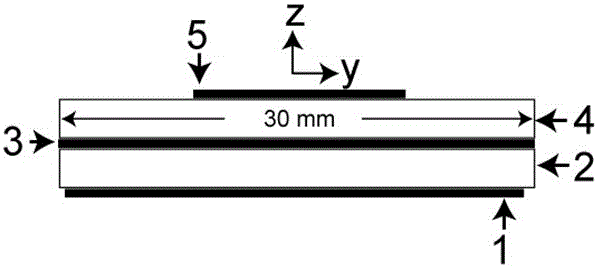
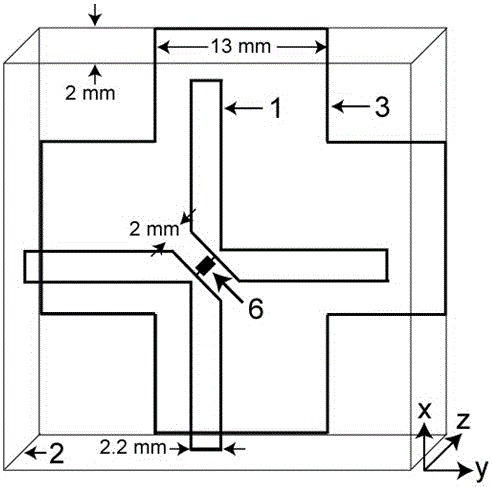
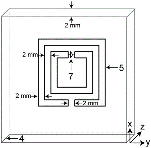
[0022] like figure 1 As shown, the wave-absorbing layer of the present invention is formed by periodic arrangement of square sub-wavelength resonant units whose unit size is less than 1 / 4 of the working wavelength. The first metal copper sheet 1, the first dielectric plate 2, the second metallic copper sheet 3, the second dielectric plate 4 and the third metallic copper sheet 5, the first metallic copper sheet 1 and the second metallic copper sheet 3 are in the shape of a cross ,like figure 2 As shown, the first metal copper sheet 1 is slotted in the middle to divide the first metal copper sheet 1 into two L-shaped slices, and a lumped resistor 6 is connected between the two metal copper slices at the slot. The first dielectric plate 2 is the same as the second dielectric plate 4, the third metal copper sheet 5 is a magnetic resonant metal copper sheet with a double-...


PUM


Abstract

The invention discloses a perfect matching wave absorbing layer composed of sub-wavelength resonance units and active circuits. The perfect matching wave absorbing layer is formed by arraying the square sub-wavelength resonance units in a periodic mode, wherein the size of each resonance unit is smaller than 1/4 work wavelength, each sub-wavelength resonance unit comprises a first metal copper piece, a first dielectric plate, a second metal copper piece, a second dielectric plate and a third metal copper piece which are overlapped in sequence, the first metal copper pieces and the second metal copper pieces are in crossed shapes, a lumped resistor is connected between two separated pieces of a slot in the middle of each first metal copper piece, the first dielectric plates and the second dielectric plates are identical, each third metal copper piece is a magnetic resonance metal copper piece with a double annular opening structure, and the inner annular opening of each third metal copper piece is connected with an active negative resistance device or the active circuit with the negative resistance property. The perfect matching wave absorbing layer is thin, low in weight, capable of realizing perfect matching absorption of electromagnetic waves with any incidence angles, and capable of being widely applied to various military and civil fields like object invisibility, antenna separation and electromagnetic shielding.

Description

technical field [0001] The invention relates to an electromagnetic wave absorbing layer, in particular to a perfectly matched wave absorbing layer formed by a sub-wavelength resonant unit and an active circuit. Background technique [0002] Electromagnetic wave absorbing material, referred to as wave absorbing material, is a functionally compatible material that can effectively absorb incident radar waves and greatly attenuate its scattering. The new generation of absorbing materials requires strong attenuation capability, wide absorption frequency band, light weight, compatibility with infrared and microwave absorption, and excellent comprehensive mechanical properties. Among them, the main application field of absorbing materials is the military field. [0003] The field of military stealth is an important application field of absorbing materials. With the rapid development of military high-tech, the detection, tracking and attack capabilities of the defense systems of al...

Claims


Application Information

Patent Timeline
Patent Type & Authority Patents(China)
IPC IPC(8): H01Q17/00
Inventor 叶德信皇甫江涛冉立新
Owner ZHEJIANG UNIV
Why Eureka
Try Eureka