Composite organic rectifier diode
A rectifier diode and composite technology, which is applied in the field of organic semiconductor electronic devices, can solve the problems of limited organic rectifier diode devices, and achieves the effects of high repeatability, simple process, and low requirements for production technology and instruments.
- Summary
- Abstract
- Description
- Claims
- Application Information
AI Technical Summary
Problems solved by technology
Method used
Image
Examples
Embodiment 1
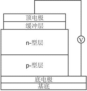
[0024] Embodiment 1: A composite organic rectifier diode device, the layers of the device are arranged in the following order from bottom to top: base, bottom electrode, p-type material layer, n-type material layer, charge buffer layer, top electrode. in:
[0025] The substrate is glass with better smoothness;
[0026] The bottom electrode is ITO photoetched on the substrate;
[0027] The p-type material layer is deposited on the bottom electrode, and the material is selected from NPB, m-MTDATA, 2T-NATA, CuPc, TPD, TAPC, or Rubrene, and its thickness is 30nm;
[0028] The n-type material layer is C deposited on the p-type material layer 60 , with a thickness of 60 nm;
[0029] The buffer layer is BCP deposited on the n-type material layer with a thickness of 7 nm;
[0030] The top electrode is metal Al deposited on the buffer layer with a thickness of 100 nm.
Embodiment 2
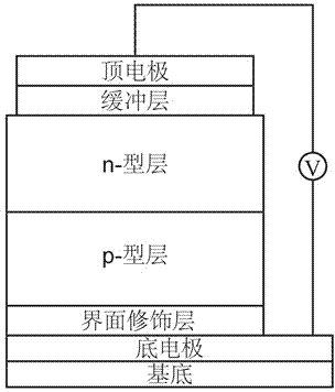
[0031] Embodiment 2: A composite organic rectifier diode device, the layers of the device are arranged in the following order from bottom to top: substrate, bottom electrode, interface modification layer, p-type material layer, n-type material layer, charge buffer layer and top electrodes, of which:
[0032] The substrate is glass with better smoothness;
[0033] The bottom electrode is ITO photoetched on the substrate;
[0034] The interface modification layer is MoO deposited on the bottom electrode 3 , with a thickness of 1 nm;
[0035] The p-type material layer is TCTA or CBP deposited on the interface modification layer, with a thickness of 30 nm;
[0036] The n-type material layer is C deposited on the p-type material layer 60 , with a thickness of 60 nm;
[0037] The charge buffer layer is BCP deposited on the n-type material layer with a thickness of 7 nm;
[0038] The top electrode is metal Al deposited on the buffer layer with a thickness of 100 nm.
Embodiment 3
[0039] Embodiment 3: A composite organic rectifier diode device, the layers of the device are arranged in the following order from bottom to top: substrate, bottom electrode, interface modification layer, p-type material layer, n-type material layer, charge buffer layer and top electrodes, of which:
[0040] The substrate is glass with better smoothness;
[0041] The bottom electrode is Al deposited on the substrate with a thickness of 50 nm;
[0042] The interface modification layer is MoO deposited on the bottom electrode 3 , with a thickness of 3 nm;
[0043] The p-type material layer is NPB, m-MTDATA, 2T-NATA, CuPc, TPD, TAPC, TCTA, CBP or Rubrene deposited on the interface modification layer, with a thickness of 30 nm;
[0044] The n-type material layer is C deposited on the p-type material layer 60 , with a thickness of 60 nm;
[0045] The charge buffer layer is BCP deposited on the n-type material layer with a thickness of 7 nm;
[0046] The top electrode is metal...
PUM
 Abstract
Description
Claims
Application Information


