Heat dissipation structure of electric device and manufacturing method thereof

A technology for electrical devices and heat dissipation structures, which is applied in the manufacture of electrical equipment components, circuit devices, printed circuits, etc., and can solve problems such as poor heat dissipation efficiency

Active Publication Date: 2018-03-16
DENSO CORP
View PDF4 Cites 0 Cited by
  • Summary
  • Abstract
  • Description
  • Claims
  • Application Information

AI Technical Summary

Problems solved by technology

In such a structure, no components are mounted on the back
Also, heat dissipation is not efficient as heat is radiated through the substrate

Method used


Image

  • Heat dissipation structure of electric device and manufacturing method thereof
  • Heat dissipation structure of electric device and manufacturing method thereof
  • Heat dissipation structure of electric device and manufacturing method thereof

Examples


no. 1 approach )

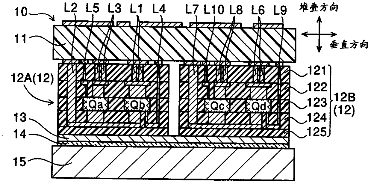
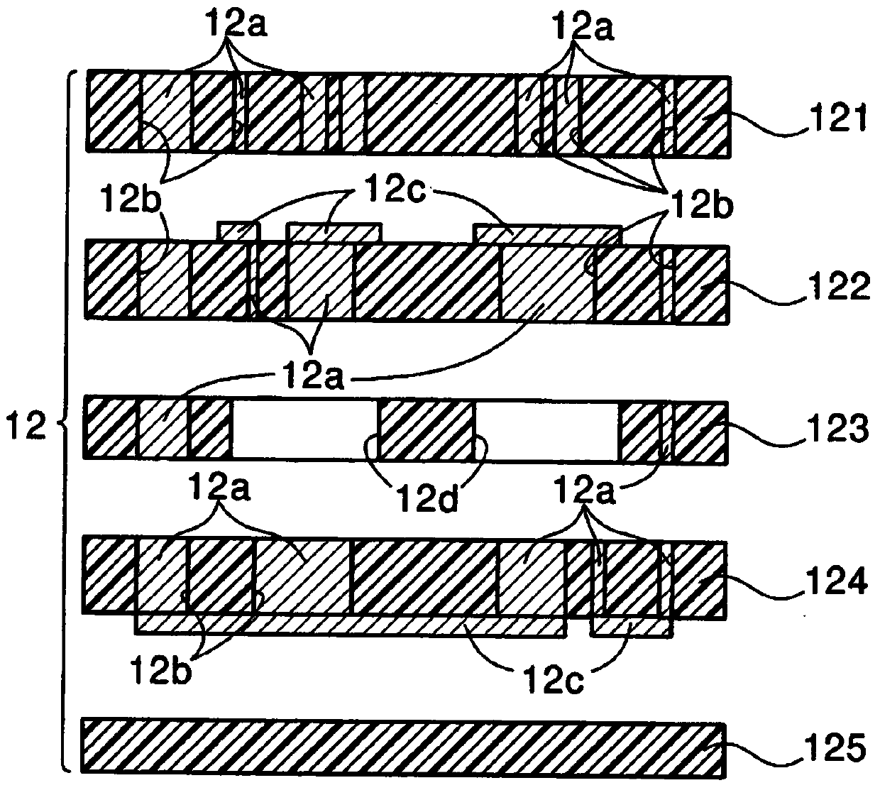
[0036] The heat dissipation structure according to the first embodiment includes a plurality of multilayer substrates between the circuit board and the heat dissipation body. will refer to Figures 1 to 8 This structure will be described. figure 1 The heat dissipation structure 10 shown in includes a circuit board 11 , a plurality of multilayer substrates 12 , a low thermal resistance element 13 , a heat conduction element 14 and a heat sink 15 . In the present embodiment, the plurality of multilayer substrates 12 includes a first multilayer substrate 12A and a second multilayer substrate 12B.

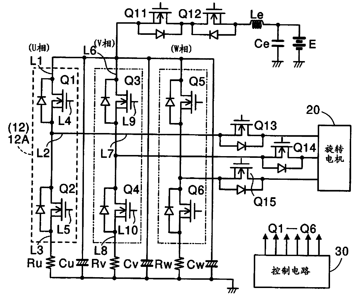
[0037] The circuit board 11 is a board on which electrical components are mounted and a conductor pattern is formed. In the present embodiment, the circuit board 11 is provided to control the rotating electric machine 20 having three phases such as U phase, V phase and W phase. Specifically, the circuit board 11 includes: a control circuit 30; resistors Rv, Ru, Rw; capacitors Cu, Cv...

no. 2 approach )

[0070] In a second embodiment, a heat dissipation structure has a multilayer substrate and electrical components located between a circuit board and a heat dissipation body. will refer to Figures 10 to 13 This structure will be described.

[0071] Figure 10 The heat dissipation structure 10 shown in the figure includes a circuit board 11 , a multilayer substrate 12 , a low thermal resistance element 13 , a heat conducting member 14 , a radiator 15 and an electrical element 16 . In this embodiment, structure 10 includes a multilayer substrate 12 and an electrical component 16 .

[0072] The multilayer substrate 12 corresponds to the substrates 12A, 12B in the first embodiment. Alternatively, the substrate 12 according to the second embodiment corresponds to the multilayer substrate according to other embodiments. The electrical elements 16 may be semiconductor devices such as switching elements, diodes, semiconductor current collectors, and integrated circuits (ICs), and / ...

no. 3 approach )

[0083] In a third embodiment, the heat dissipation structure includes a plurality of electrical components located between the circuit board and the heat dissipation body. will refer to Figures 14 to 16 This structure will be described.

[0084] Figure 14 The heat dissipation structure 10 shown in includes a circuit board 11 , a low thermal resistance element 13 , a heat conducting member 14 , a heat sink 15 , and a plurality of electrical components 16 . In the present embodiment, the plurality of electrical components 16 include a first electrical component 16A and a second electrical component 16B.

[0085] The electrical elements 16A, 16B correspond to the electrical element 16 and / or other electrical devices according to the second embodiment. The electrical elements 16A, 16B may be semiconductor devices such as switching elements, diodes, semiconductor current collectors, and integrated circuits (ICs), and / or resistors, capacitors, coils, reactors, and the like. El...


PUM


Abstract

A heat dissipation structure for an electrical device (Qa‑Qd, 16), comprising: at least one multilayer substrate (12, 12A, 12B) comprising a conductor pattern (12c) and made of an insulating material A plurality of base parts (121‑125) formed, the conductor pattern and the plurality of base parts are stacked into a multi-layer structure to electrically connect the conductor pattern and the interlayer connection (L1‑L10) in the base part; the electrical device has At least one of a first electrical component (Qa-Qd) built into at least one multilayer substrate and a second electrical component (16) not built into the multilayer substrate; and a low thermal resistance component opposite to the electrical device ( 13). Low thermal resistance components have lower thermal resistance than insulating materials.

Description

technical field [0001] The present disclosure relates to a heat dissipation structure of an electrical device, which is used for heat dissipation of electrical components; and to a method for manufacturing the heat dissipation structure. Background technique [0002] Generally, a technique related to a multilayer substrate having excellent heat dissipation characteristics of semiconductor elements and having low manufacturing cost is disclosed in, for example, JP-A-2004-158545. The multilayer substrate includes heat dissipation plates disposed on both sides in an up-down direction and insulated from the semiconductor elements. [0003] However, in the heat dissipation structure of semiconductor elements such as MOS-FETs (ie, Metal Oxide Semiconductor Field Effect Transistors) that provide motor drive circuits, for example, between bare chips and SMDs (ie, surface mount devices) including package structures Such surface mount components are mounted on the surface of the subs...

Claims


Application Information

Patent Timeline
Patent Type & Authority Patents(China)
IPC IPC(8): H01L23/34H05K7/20H05K1/02
CPCH05K7/209H01L2924/0002H05K3/4614H02M7/003H05K1/0265H05K1/185H05K2201/10166H01L23/3677H01L23/3735H01L23/5389Y10T29/49165Y10T29/49139Y10T29/49155Y10T29/49126H05K3/0058H01L2924/00H05K7/2039H05K3/10H05K3/22H05K3/303
Inventor 山中隆广原芳道山本敏久龟山浩二小林裕次
Owner DENSO CORP
Why Eureka
Try Eureka