Array panel and manufacturing method thereof
一种阵列面板、制作方法的技术,应用在仪器、半导体器件、光学等方向,能够解决耗费电能、降低显示质量、电压无法达到预期值等问题,达到降低功耗、降低电量消耗的效果
- Summary
- Abstract
- Description
- Claims
- Application Information
AI Technical Summary
Problems solved by technology
Method used
Image

Examples
Embodiment Construction
[0026] The following descriptions of the various embodiments refer to the accompanying drawings to illustrate specific embodiments in which the present invention can be practiced.
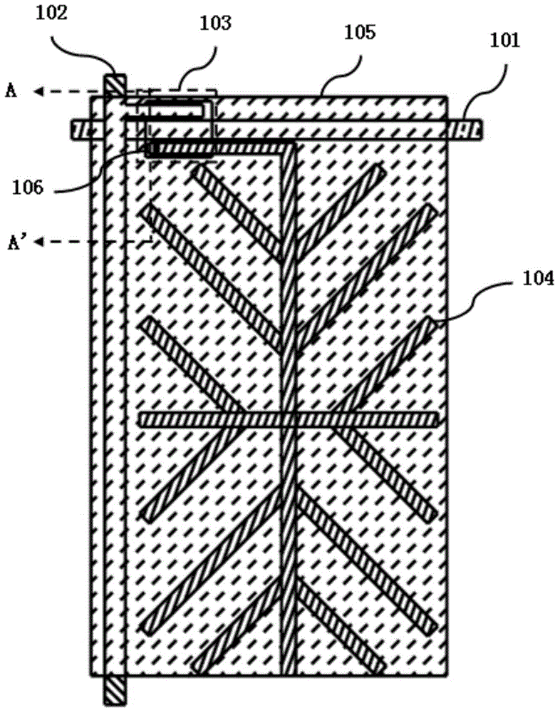
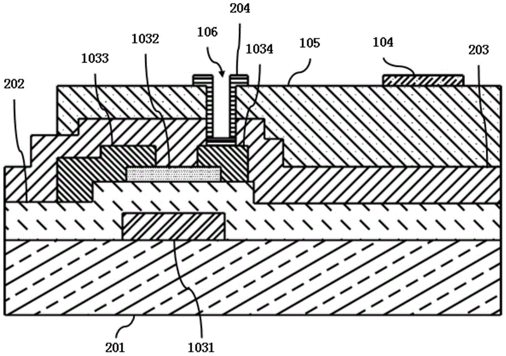
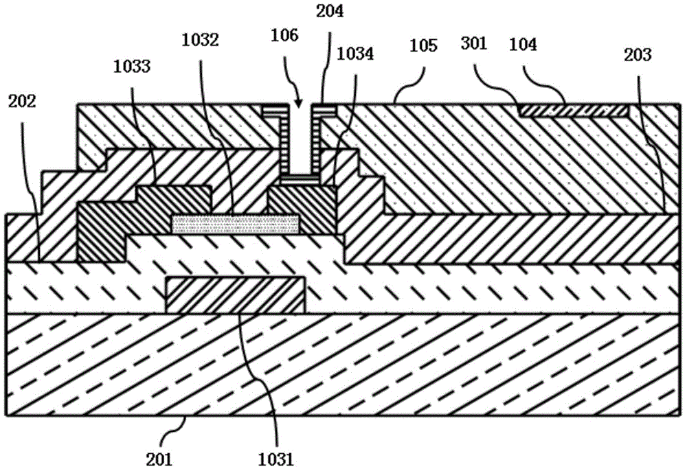
[0027] refer to figure 1 with figure 2 , figure 1 It is a schematic diagram of the pixel unit in the array panel of the present invention. figure 2 for figure 1 Schematic diagram of the first embodiment of the section A-A' in the middle.
[0028] The array panel of this embodiment includes a substrate 201 , a pixel array, at least one scan line 101 and at least one data line 102 . Wherein, the scan lines 101 , the data lines 102 and the pixel array are all disposed on the substrate 201 .
[0029] The pixel array includes at least one pixel unit, wherein the pixel unit includes a thin film transistor 103 , a pixel electrode 104 and a color film (Color Film / Color Filter) layer 105 . The color filter layer 105 is disposed between a first plane and a second plane, wherein the first plane is the...
PUM
 Abstract
Description
Claims
Application Information
 - R&D
- Intellectual Property
- Life Sciences
- Materials
- Tech Scout
- Unparalleled Data Quality
- Higher Quality Content
- 60% Fewer Hallucinations
Browse by: Latest US Patents, China's latest patents, Technical Efficacy Thesaurus, Application Domain, Technology Topic, Popular Technical Reports.
© 2025 PatSnap. All rights reserved.Legal|Privacy policy|Modern Slavery Act Transparency Statement|Sitemap|About US| Contact US: help@patsnap.com