Method and system for 2D/3D microstructure texture decoration on surface of raw material
A microstructure texture, 2D\3D technology, applied in the field of image processing, can solve the problems of technical process blockade, long, must be completed at one time, transfer, etc., to achieve the effect of simple production equipment, low development cost, and short development cycle
- Summary
- Abstract
- Description
- Claims
- Application Information
AI Technical Summary
Problems solved by technology
Method used
Image
Examples
Embodiment Construction
[0026] The specific implementation manners of the present invention will be further described in detail below in conjunction with the accompanying drawings and embodiments. The following examples are used to illustrate the present invention, but are not intended to limit the scope of the present invention.
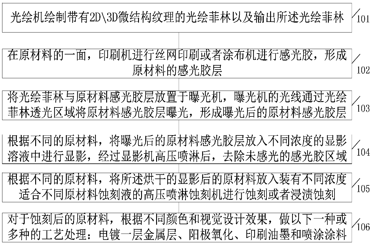
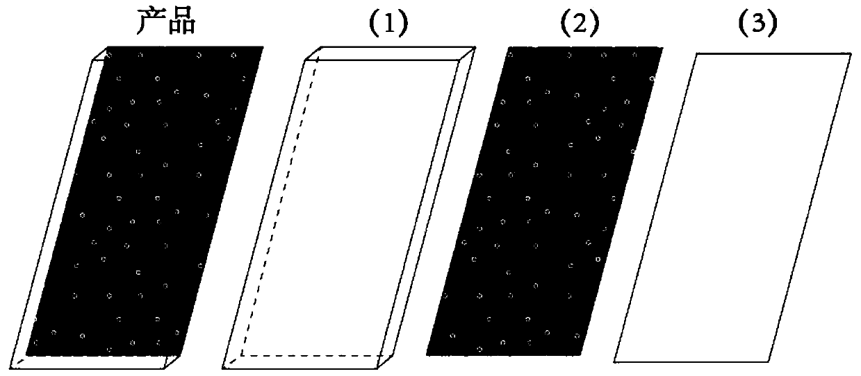
[0027] see figure 1 and figure 2 As shown, a method for 2D\3D microstructure texture decoration on the surface of raw materials, including
[0028] Step 101: A high-precision photoplotter draws a photopainted film with an accuracy of 25400dpi and outputs the photopainted film. The photopainted film is as follows: figure 2 as shown in (2).
[0029] For example: the photopainting film microstructure texture can be combined from a line width of 0.01mm to a line width of 0.08mm. The precision of the high-precision photoplotter is 25400DPI, and the resolution of the output photopainting film is 25400DPI.
[0030] Step 102: On one side of the raw material, the printing mac...
PUM
 Abstract
Description
Claims
Application Information


