Method for determining photoetching process window online

A lithography process and technology, applied in microlithography exposure equipment, photolithography process exposure devices, etc., can solve the problems of inability to accurately judge the size of the difference, increase time and cost, and consume labor, so as to shorten the judgment and adjustment cycle. , Improve the quality and reduce the effect of misjudgment

Active Publication Date: 2014-08-20
SHANGHAI HUALI MICROELECTRONICS CORP
View PDF5 Cites 6 Cited by
  • Summary
  • Abstract
  • Description
  • Claims
  • Application Information

AI Technical Summary

Problems solved by technology

[0006] However, those skilled in the art know that in the current online operation process, through human analysis and judgment, it is impossible to accurately determine the difference between the critical dimension in the graphic and the target critical dimension, and it is not easy to determine the specific position of the graphic when it is etched on the wafer. It is also impossible to establish a specific correspondence between focal length, energy, and key dimensions, so data such as energy gradient, available focal depth, optimal energy, and optimal focal length cannot be determined; and it increases the time cost of judgment and consumes manpower

Method used


Image

  • Method for determining photoetching process window online
  • Method for determining photoetching process window online
  • Method for determining photoetching process window online

Examples


Embodiment Construction

[0035] Attached below Figure 2-4 , the specific embodiment of the present invention will be further described in detail.

[0036] It should be noted that in the following embodiments, the target critical dimension is 55nm and the specification is + / -6nm as an example.

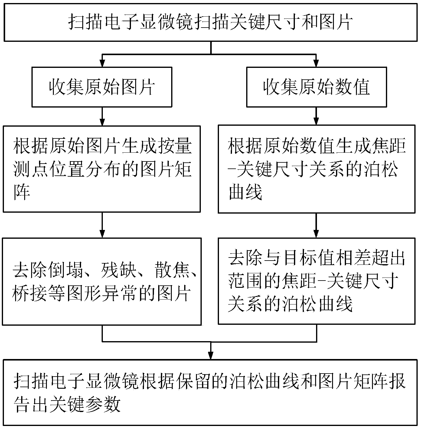
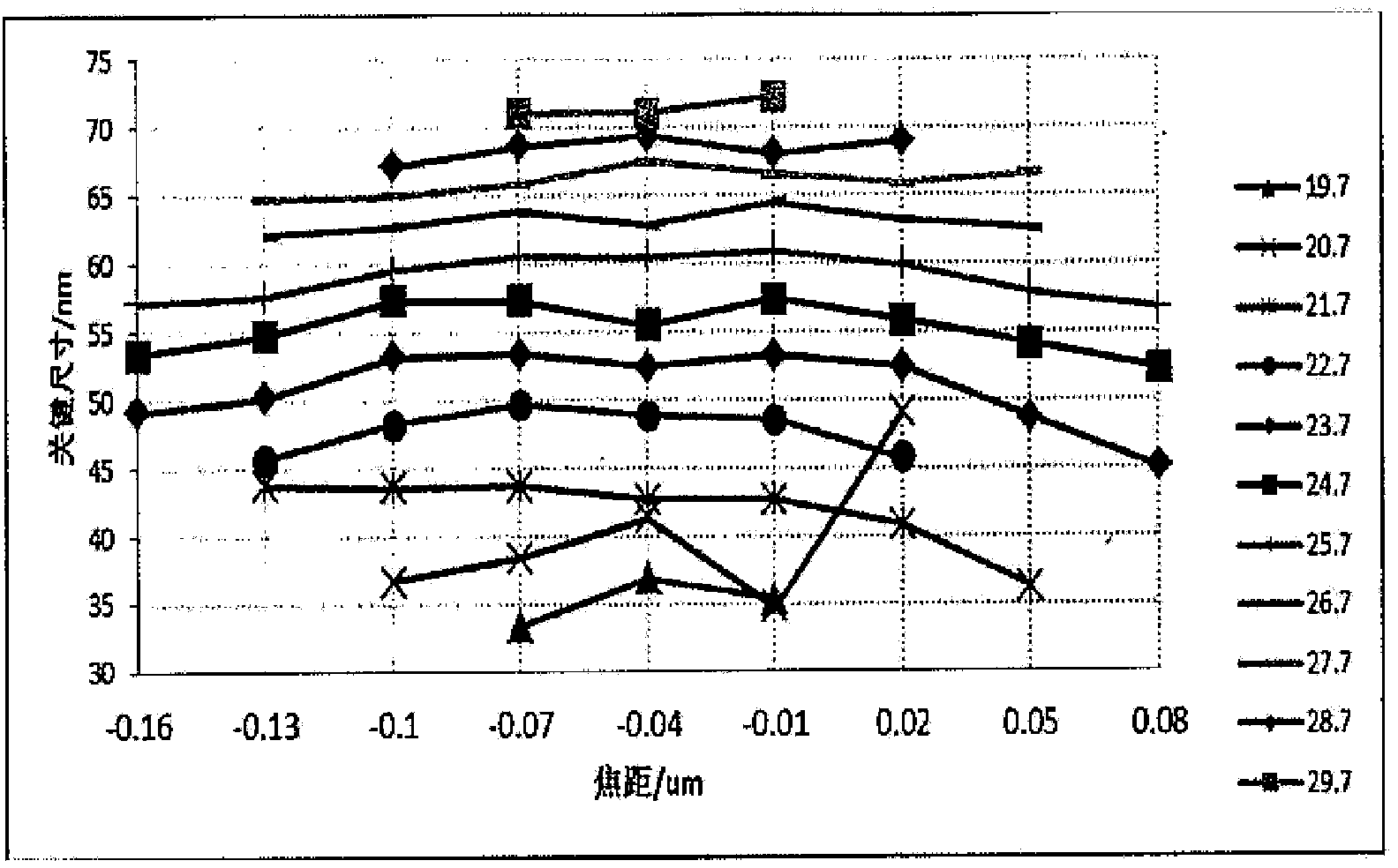
[0037] see figure 2 , figure 2 It is a logical control block diagram for scanning a wafer with a scanning electron microscope and performing data processing in the present invention; it illustrates a method for determining the photolithography process window on-line, including the following steps:

[0038] Step S1: Please refer to Table 1. Table 1 is the focal length-energy matrix collected by a scanning electron microscope. The target critical dimension is 55nm, and the specification is + / -6nm. As shown in Table 1, the first row of the matrix is ​​energy, and the unit is mj / cm 2 , increasing 1mj / cm for each cell from left to right 2 ;The first column of the matrix is ​​the focal length, the unit is um,...


PUM


Abstract

The invention discloses a method for determining a photoetching process window online. The method comprises the steps: measuring a key size of a surface pattern of the wafer through a scanning electron microscope and generating data; generating Poisson curves and a picture matrix by the scanning electron microscope according to the measured data, then eliminating unavailable Poisson curves and remaining available Poisson curves, rejecting unqualified pictures such as pattern collapse and remaining qualified pictures; and finally, rapidly and accurately reporting an energy gradient, an available focal depth, an optimal energy and an optimal focal length by the scanning electron microscope according to the selected Poisson curves and the picture matrix. According to the method, judgment and regulation periods of key parameters in the photoetching process can be shortened, the purpose of rapidly and accurately determining the size of the optimal photoetching process window is realized, the time of obtaining the photoetching process window is shortened, and the quality of a photoetching pattern is improved.

Description

technical field [0001] The invention relates to the technical field of integrated circuit manufacturing, in particular to a method for determining a photolithographic process window in a semiconductor device manufacturing process. Background technique [0002] With the development of photolithography process in the manufacturing technology of integrated circuit semiconductor devices, integrated circuits are developing in the direction of small size, low power consumption and low cost, and the time cost of manufacturing integrated circuits is an important consideration. The lithography process is an important part of the integrated circuit manufacturing process. The lithography process is to use a lithography machine to etch and prepare small-scale graphic structures on the wafer. The part protected by the glue is removed by physical or chemical methods, so as to achieve the purpose of transferring the pattern on the photomask to the substrate; with the reduction of the volum...

Claims


Application Information

Patent Timeline
Patent Type & Authority Applications(China)
IPC IPC(8): G03F7/20
Inventor 李中华毛智彪甘志锋
Owner SHANGHAI HUALI MICROELECTRONICS CORP
Why Eureka
Try Eureka