
Methods of fabricating dilute nitride semiconductor materials for use in photoactive devices and related structures

一种光敏器件、制造方法的技术,应用在半导体/固态器件制造、半导体器件、半导体激光器等方向,能够解决III-V族半导体材料商用规模难以制造等问题

Active Publication Date: 2014-08-20
SOITEC SA
View PDF5 Cites 0 Cited by
  • Summary
  • Abstract
  • Description
  • Claims
  • Application Information

AI Technical Summary

Problems solved by technology

[0007] Such dilute nitride III-V semiconductor materials have proven difficult to fabricate, at least on a commercial scale

Method used


Image

  • Methods of fabricating dilute nitride semiconductor materials for use in photoactive devices and related structures
  • Methods of fabricating dilute nitride semiconductor materials for use in photoactive devices and related structures
  • Methods of fabricating dilute nitride semiconductor materials for use in photoactive devices and related structures

Examples


Embodiment approach

[0050] Additional non-limiting embodiments of the present invention are as follows:

Embodiment approach 1

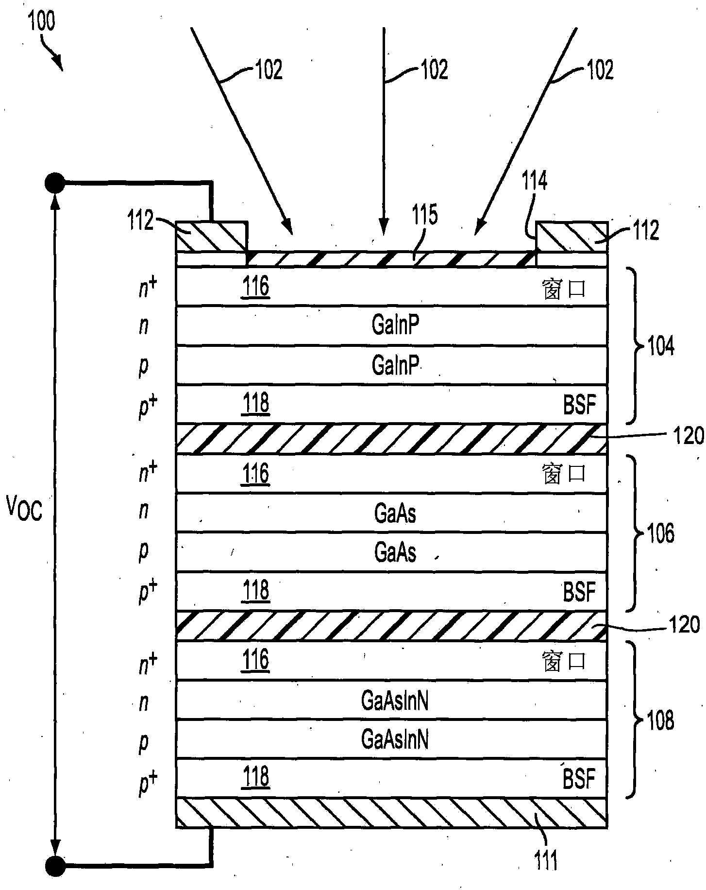
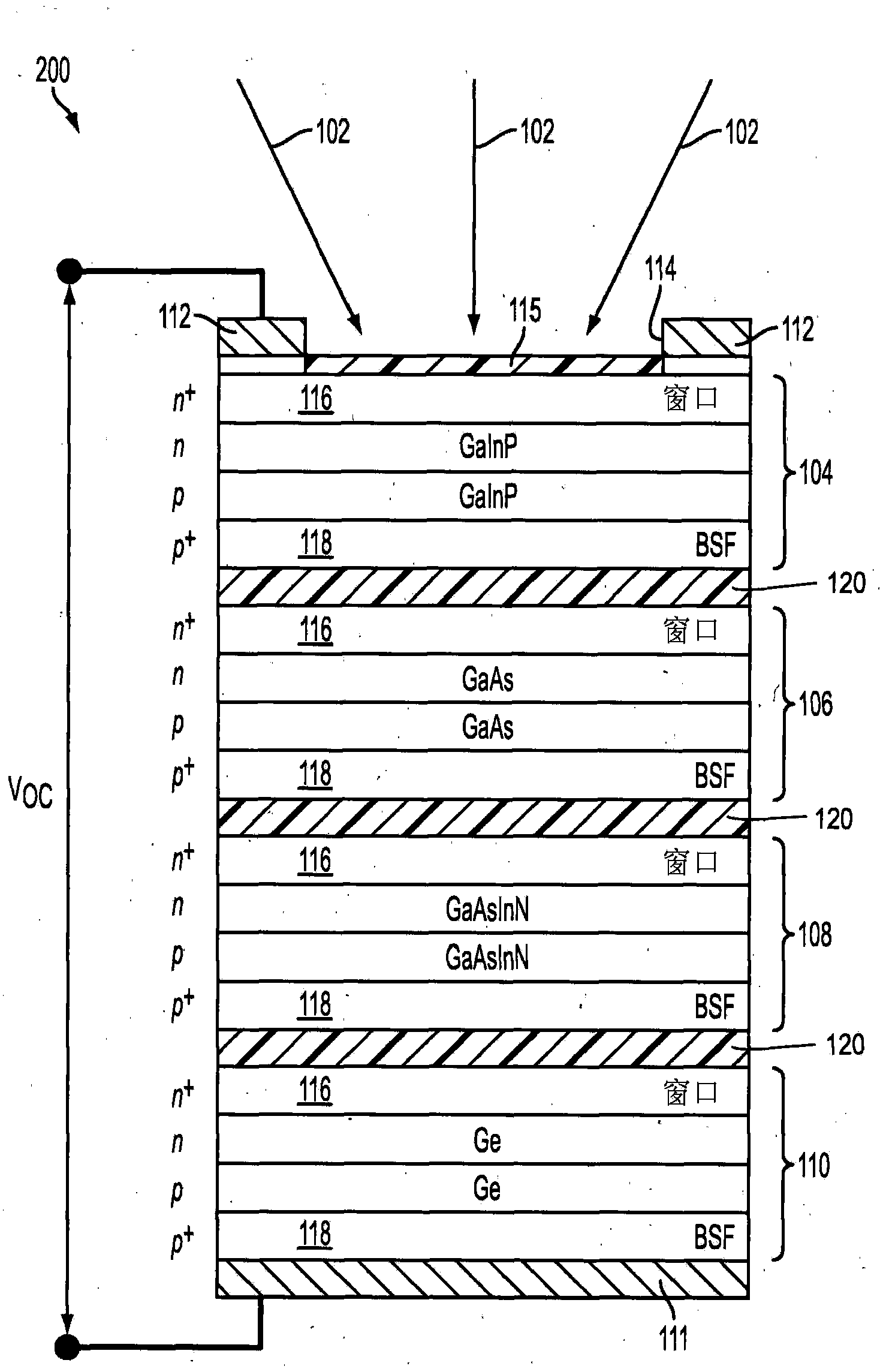
[0051] Embodiment 1: A method for manufacturing a photosensitive device, comprising: forming GaInN on a substrate in a chamber; and replacing part of N atoms in GaInN with As atoms to convert at least a part of GaInN into GaInNAs.

Embodiment approach 2

[0052] Embodiment 2: The method of Embodiment 1, wherein the step of substituting As atoms for some N atoms in GaInN includes heating GaInN in the presence of an arsenic-containing gas or vapor in a chamber.


PUM

PropertyMeasurementUnit
band gapaaaaaaaaaa
band gapaaaaaaaaaa
band gapaaaaaaaaaa

Abstract

Dilute nitride III-V semiconductor materials may be formed by substituting As atoms for some N atoms within a previously formed nitride material to transform at least a portion of the previously formed nitride into a dilute nitride III-V semiconductor material that includes arsenic. Such methods may be employed in the fabrication of photoactive devices, such as photovoltaic cells and photoemitters. The methods may be carried out within a deposition chamber, such as a metalorganic chemical vapor deposition (MOCVD) or a vapor phase epitaxy (HVPE) chamber.

Description

technical field [0001] Embodiments of the present invention generally relate to methods of fabricating dilute nitride III-V semiconductor materials for photoactive devices, methods of fabricating photoactive devices including dilute nitride III-V semiconductor materials, and methods utilizing the dilute nitride III-V semiconductor materials. formed photosensitive device. Background technique [0002] Photosensitive devices are semiconductor devices that use semiconductor materials to convert electromagnetic radiation into electrical energy or convert electrical energy into electromagnetic radiation. Photosensitive devices include, for example, photovoltaic cells, light emitting diodes, and laser diodes. [0003] Photovoltaic cells (also referred to in this field as "solar cells" or "photovoltaic cells") are used to convert energy from light (eg, sunlight) into electricity. Photovoltaic cells typically include one or more pn junctions and can be fabricated from conventional...

Claims


Application Information

Patent Timeline
Patent Type & Authority Applications(China)
IPC IPC(8): H01L21/02H01L31/0687H01L33/32
CPCH01L31/0687H01L33/32H01L33/08H01L21/0242H01L21/02664H01L21/0254H01S5/32358H01L31/03048H01L33/0062H01L21/0262H01L31/1848H01L21/02546H01S5/32341Y02E10/544H01L27/153H01L21/02458
Inventor 尚塔尔·艾尔纳R·斯科特C·卡尼扎瑞斯
Owner SOITEC SA
Learn More