Check patentability & draft patents in minutes with Patsnap Eureka AI!

Pixel structure

A pixel structure and pixel technology, applied in nonlinear optics, instruments, optics, etc., can solve the problems affecting the display effect of the display panel and the liquid crystal use efficiency of the liquid crystal layer, and achieve the effect of reducing the driving voltage and improving the use efficiency

Active Publication Date: 2014-08-27
AU OPTRONICS CORP
View PDF4 Cites 0 Cited by
  • Summary
  • Abstract
  • Description
  • Claims
  • Application Information

AI Technical Summary

Problems solved by technology

Since the liquid crystal is driven by an electric field, the distribution of electrodes on both sides of the liquid crystal layer affects the efficiency of the liquid crystal in the liquid crystal layer, and the efficiency of the liquid crystal will affect the display effect of the display panel

Method used


Image

  • Pixel structure
  • Pixel structure
  • Pixel structure

Examples


Embodiment Construction

[0038] In order to make the above-mentioned features and advantages of the present invention more comprehensible, specific implementations are given below and described in detail with accompanying drawings.

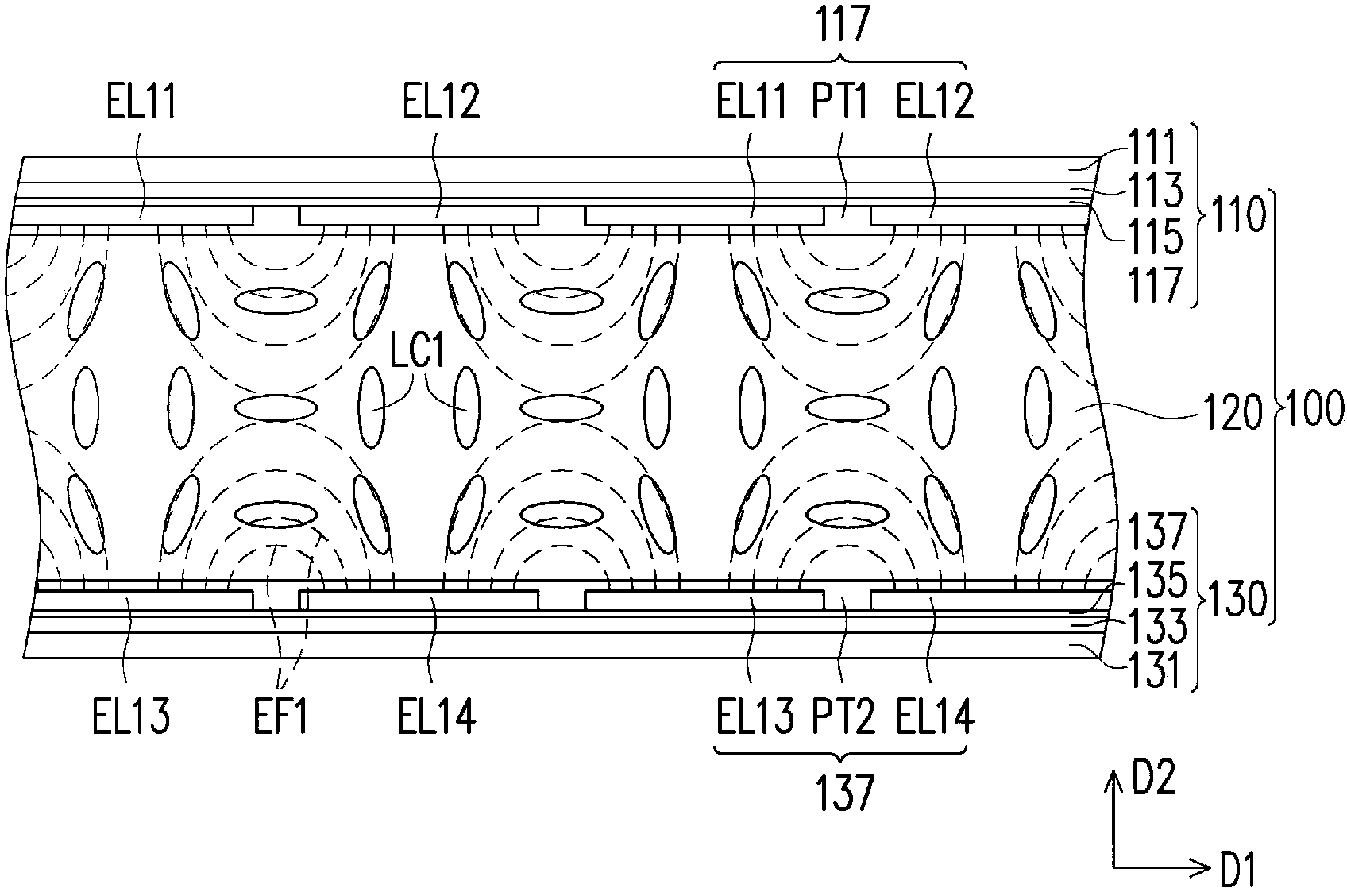
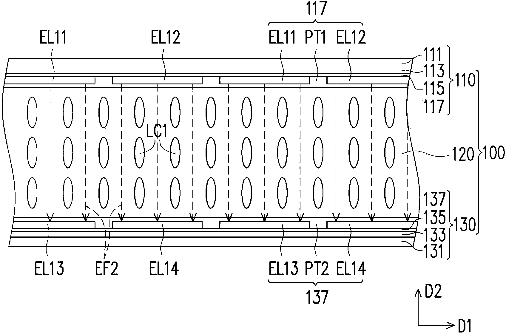
[0039] Figure 1A to Figure 1D It is a driving schematic diagram of a pixel structure according to an embodiment of the present invention. Please refer to Figure 1A , in this embodiment, the pixel structure 100 includes an upper substrate 110, a liquid crystal layer 120 and a lower substrate 130, wherein the liquid crystal layer 120 is located between the upper substrate 110 and the lower substrate 130, that is, the liquid crystal layer 120 is disposed on the electrode layers 117 and 137 Among them, the liquid crystal layer 120 includes a plurality of liquid crystal molecules, the liquid crystal molecules can be bistable liquid crystal molecules, cholesteric liquid crystal molecules, and the cholesteric liquid crystal molecules are liquid crystal molecules of polymer st...


PUM


Abstract

A pixel structure comprises a first electrode layer, a second electrode layer and a liquid crystal layer. The first electrode layer comprises a plurality of first electrodes and a plurality of second electrodes. The first electrodes are used for receiving first driving voltages. The second electrodes are used for receiving second driving voltages. The second electrode layer comprises a plurality of third electrodes and a plurality of fourth electrodes. The third electrodes are used for receiving third driving voltages. The fourth electrodes are used for receiving fourth driving voltages. The liquid crystal layer is arranged between the first electrode layer and the second electrode layer. The first electrodes and the second electrodes are arranged in an alternate way along a first direction parallel to the liquid crystal layer. The third electrodes and the fourth electrodes are alternately arranged along a direction parallel to the first direction.

Description

technical field [0001] The invention relates to a pixel structure, in particular to a liquid crystal pixel structure. Background technique [0002] With the advancement of semiconductor components and display devices, multimedia technology has become quite developed. As far as displays are concerned, thin film transistor liquid crystal displays have gradually become the mainstream of the market due to their superior characteristics such as high image quality, good space utilization efficiency, low power consumption, and no radiation. Generally speaking, a thin film transistor liquid crystal display panel is mainly composed of a thin film transistor array substrate, a color filter substrate, and a liquid crystal layer sandwiched between the two substrates. Since the liquid crystal has a structure driven by an electric field, the distribution of electrodes on both sides of the liquid crystal layer affects the efficiency of using the liquid crystal in the liquid crystal layer,...

Claims


Application Information

Patent Timeline
Patent Type & Authority Applications(China)
IPC IPC(8): G02F1/1343G02F1/133
CPCG09G3/3629G09G3/3614G09G2310/061
Inventor 白宗纬曾衡逸吴育庆徐文浩林宗贤李承璋
Owner AU OPTRONICS CORP
Features
  • R&D
  • Intellectual Property
  • Life Sciences
  • Materials
  • Tech Scout
  • Unparalleled Data Quality
  • Higher Quality Content
  • 60% Fewer Hallucinations
Learn More