
Integrated passive device wafer-level packaging three-dimensional stacked structure and manufacturing method

A technology for integrating passive devices and wafer-level packaging, which is applied in semiconductor/solid-state device manufacturing, electric solid-state devices, semiconductor devices, etc., can solve problems such as low integration and non-integration of passive passive devices, and achieve good stress buffering Protective effect, improve electrical quality, and improve cost performance

Active Publication Date: 2014-08-27
NAT CENT FOR ADVANCED PACKAGING
View PDF8 Cites 12 Cited by
  • Summary
  • Abstract
  • Description
  • Claims
  • Application Information

AI Technical Summary

Problems solved by technology

[0004] In the prior art, the biggest disadvantage of wafer-level chip packaging and thin-film integrated passive devices is the low degree of integration
In general, wafer-level chip packaging does not integrate passive passive devices, and the matching passive devices occupy about 80% of the circuit board area and 70% of the product assembly cost

Method used


Image

  • Integrated passive device wafer-level packaging three-dimensional stacked structure and manufacturing method
  • Integrated passive device wafer-level packaging three-dimensional stacked structure and manufacturing method
  • Integrated passive device wafer-level packaging three-dimensional stacked structure and manufacturing method

Examples


Embodiment Construction

[0024] The present invention will be further described below in conjunction with specific drawings.

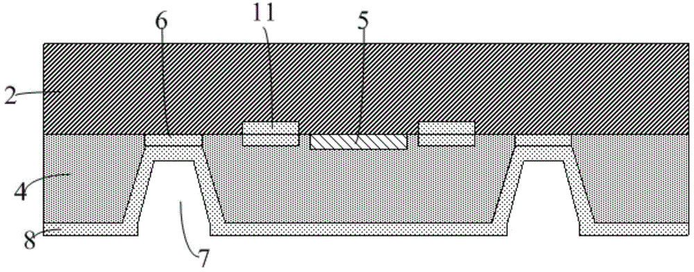
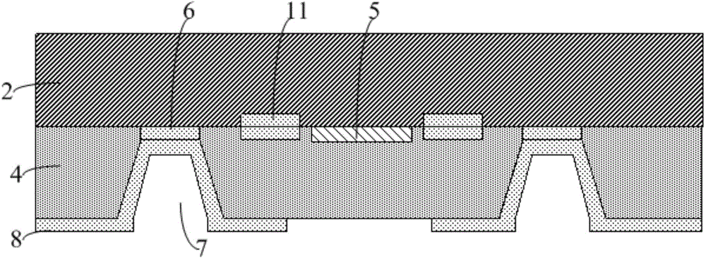
[0025] Such as Image 6 As shown: the integrated passive device wafer level package three-dimensional stack structure includes PCB board 1, wafer level package chip 2, IPD chip 3, glass substrate 4, IPD device 5, metal wiring layer 6, TGV hole 7, back Metal wiring layer 8, pad 9, solder ball 10, chip signal port 11, etc.

[0026] Such as Image 6 As shown, the three-dimensional stacked structure of the present invention is packaged on a PCB board 1, including a wafer-level packaging chip 2 and an IPD chip 3; the IPD chip 3 includes a glass substrate 4, and an IPD device 5 and Connect the metal wiring layer 6 of the IPD device 5, the IPD device 5 and the metal wiring layer 6 are flush with the front of the IPD chip 1, and the metal wiring layer 6 is connected to the chip signal port 11 of the wafer-level packaging chip 2; on the glass substrate The backside of 4 is etched to...


PUM


Abstract

The invention relates to an integrated passive device wafer-level packaging three-dimensional stacked structure and a manufacturing method. The integrated passive device wafer-level packaging three-dimensional stacked structure comprises a wafer-level packaging chip and an IPD chip. The IPD chip comprises a glass substrate, wherein an IPD device and a metal wiring layer are arranged on the front surface of the glass substrate, the back surface of the glass substrate is etched to form TGV holes, back surface metal wiring layers are arranged on the back surface of the glass substrate and the inner surfaces of the TGV holes, a welding ball is arranged on a welding pad of each back surface metal wiring layer, and the welding balls are connected with a PCB. The manufacturing method of the three-dimensional stacked structure comprises the following steps that (1) the wafer-level packaging chip and the IPD chip of the glass substrate are stacked; (2) the back surface of the IPD chip is etched to form the TGV holes, the back surface metal wiring layer is manufactured on the back surface of the glass substrate; (3) the back surface metal wiring layer is etched into two insulated parts; the welding pads and welding balls are manufactured on the two parts of the back surface metal wiring layer, and the welding balls are connected with the PCB. By means of the integrated passive device wafer-level packaging three-dimensional stacked structure and the manufacturing method, short-distance interconnection between the chip and the IPD device is achieved, and the electric quality is improved.

Description

technical field [0001] The invention relates to a three-dimensional stacking structure of wafer-level packaging, in particular to a three-dimensional stacking structure of wafer-level packaging of integrated passive devices and a manufacturing method thereof, belonging to the technical field of high-density electronic packaging. Background technique [0002] The difference between wafer-level packaging and traditional packaging methods is that traditional chip packaging is cut first and then packaged and tested. The area after packaging is at least 20% larger than the original chip size; while wafer-level packaging is first on the entire wafer. Carry out packaging and testing, and then dicing and segmentation. Therefore, the volume after packaging is the same as the size of the bare chip, which can greatly reduce the size of the chip after packaging. Wafer-level chip packaging provides low-cost, high-performance integrated packaging that can replace the current bonded BGA (B...

Claims


Application Information

Patent Timeline
Patent Type & Authority Applications(China)
IPC IPC(8): H01L23/488H01L21/60H01L25/16
CPCH01L2224/10
Inventor 何洪文孙鹏
Owner NAT CENT FOR ADVANCED PACKAGING
Learn More