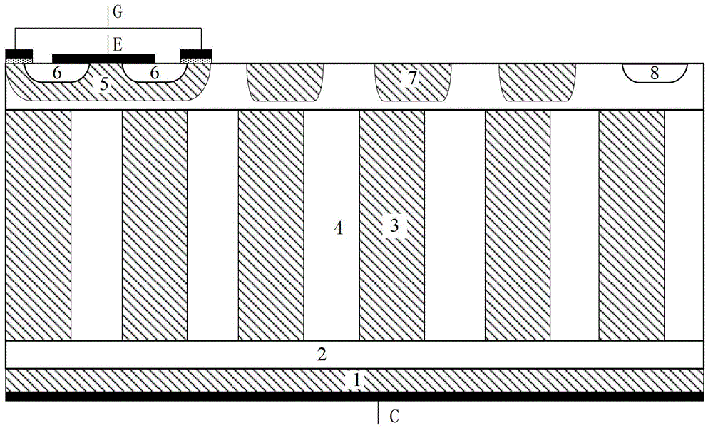
Insulated gate bipolar transistor and manufacturing method
A technology of bipolar transistors and insulated gates, applied in semiconductor/solid-state device manufacturing, semiconductor devices, electrical components, etc., can solve the problems that cannot meet the requirements of IGBT reverse withstand voltage capability
- Summary
- Abstract
- Description
- Claims
- Application Information
AI Technical Summary
Problems solved by technology
Method used
Image
Examples
Embodiment 1
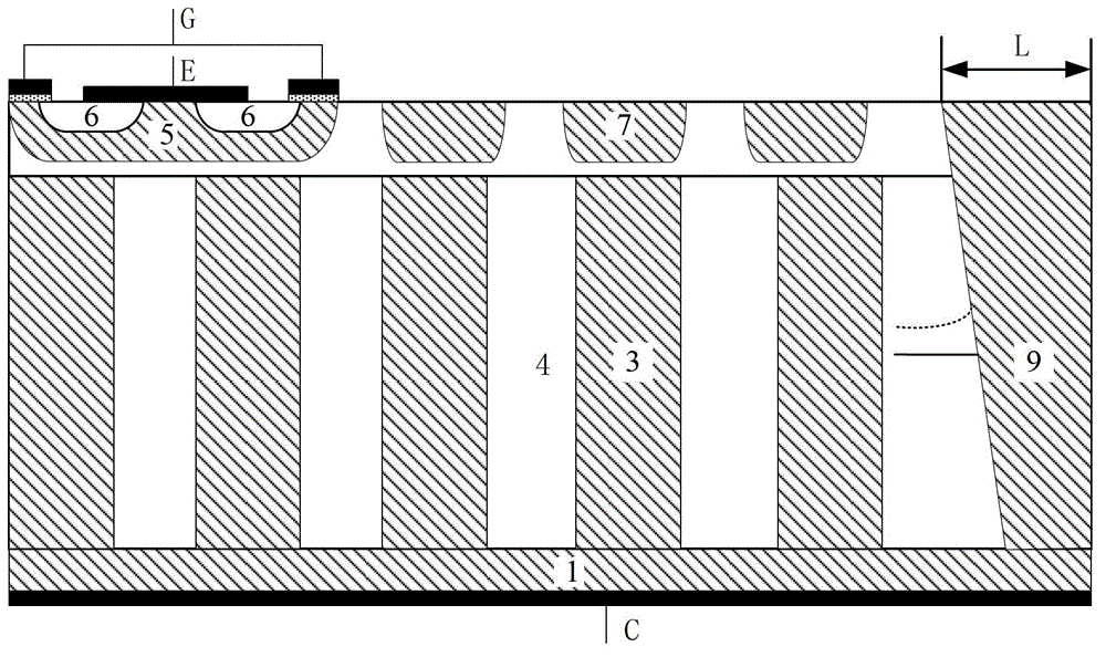
[0078] This embodiment provides an IGBT, the IGBT is provided with a second terminal structure, and the second terminal structure serves as a reverse withstand voltage terminal structure of the IGBT, which can effectively improve the ability of the IGBT to withstand reverse withstand voltage.
[0079] refer to figure 2 , figure 2 A schematic structural diagram of an IGBT provided in this embodiment, including:
[0080] P-type collector area 1;
[0081] A super-junction drift region disposed on the surface of the P-type collector region 1, the super-junction drift region includes a plurality of P-type regions 3 and N-type regions 4 arranged at intervals in the lateral direction;
[0082] An active region located on the surface of the super junction drift region and a first terminal structure, the first terminal structure surrounds the active region; wherein the active region includes: a plurality of IGBT cells, figure 2 Only one IGBT cell is shown in the figure, including...
Embodiment 2
[0090] In the above embodiments, the second terminal structure of the IGBT is integrally formed, and the second terminal structure is formed at one time by using an ion implantation process. However, the second terminal structure of the integrally formed structure has higher requirements on the manufacturing process and requires greater injection energy.
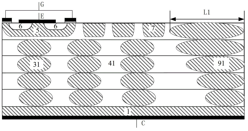
[0091]The inventors found that the non-integrated second terminal structure can be formed through multiple epitaxy and implantation processes, so as to reduce the manufacturing cost of the IGBT. The second terminal structure of the non-integrated structure means that the second terminal structure is formed in a multi-layer silicon layer after multiple epitaxy, and is not formed on a whole silicon substrate.
[0092] refer to image 3 , on the basis of the above embodiments, this embodiment provides another IGBT, which has a P-type second terminal structure 91 that is not integrally formed.
[0093] In the longitudinal sect...
Embodiment 3
[0113] Based on the above embodiments, this embodiment provides another IGBT, refer to Figure 9 , in the longitudinal section, the IGBT has a P-type second terminal structure 92 that is not integrally formed. The P-type second terminal structure 92 includes: a plurality of rectangular regions stacked in the first direction, and the widths of the plurality of rectangular regions increase in the first direction, so that the width of the P-type second terminal structure 92 L2 is incremented in the first direction.
[0114] The super junction drift region of the IGBT includes: a plurality of P-type regions 32 and N-type regions 42 , and the P-type regions 32 and N-type regions 42 are distributed at intervals. In the above longitudinal section, the P-type region 32 is rectangular, so that its width in the first direction does not change.
[0115] The second terminal structure 92 of the IGBT in this embodiment can be formed at the same time as its superjunction drift region, and ...
PUM
 Abstract
Description
Claims
Application Information


