High-speed photoelectric conversion device and assembly method thereof

A photoelectric conversion device, high-speed technology, applied in the coupling of optical waveguide, etc., can solve the problems of limiting high-frequency signal transmission, large inductance on the line, etc., to avoid signal attenuation, increase the transmission rate, and save costs.

Inactive Publication Date: 2016-01-13
昆山柯斯美光电有限公司
View PDF6 Cites 0 Cited by
  • Summary
  • Abstract
  • Description
  • Claims
  • Application Information

AI Technical Summary

Problems solved by technology

Due to the limitations of PCB board manufacturing technology (usually the line width and line spacing is 4mil / 4mil), and the arc of the wire, the distance from the driver circuit chipset to the VCSEL chip array and PD chip array often exceeds 1mm, while 10Gbps or above The length of the transmission signal bonding should not exceed 1mm, otherwise the inductance of the line will be relatively large, thus limiting the transmission of high-frequency signals

Method used


Image

  • High-speed photoelectric conversion device and assembly method thereof
  • High-speed photoelectric conversion device and assembly method thereof
  • High-speed photoelectric conversion device and assembly method thereof

Examples


Embodiment Construction

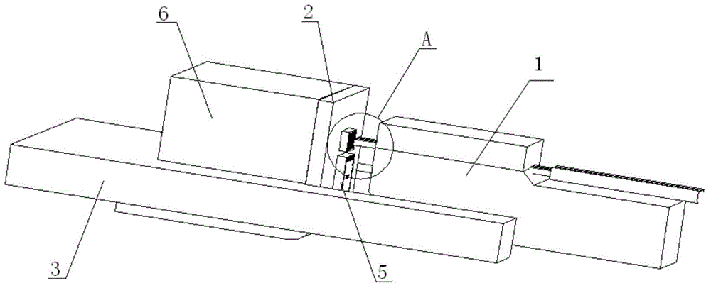
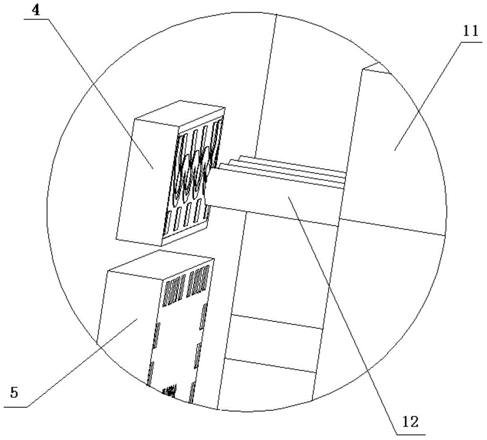
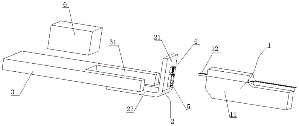
[0030] Such as figure 1 , figure 2 with image 3 As shown, a high-speed photoelectric conversion device includes an optical fiber array assembly 1, a flexible wire board 2, a PCB circuit board 3, a photoelectric chip array group 4 (such as a VCSEL chip array or / and a PD chip array), and is used to drive the The driving circuit chipset 5 and the stopper 6 of the photoelectric chip array group; the optical fiber array assembly includes a fixed seat 11 and multiple parallel optical fibers 12 that are spaced and positioned in the fixed seat; the PCB circuit board One side has a U-shaped notch 31, and the flexible cord board includes a mounting part 21 and a welding part 22 that are integrally bent at a set angle. Blocked in the notch, the welding part is attached to the bottom of the stopper and extends to the bottom of the PCB circuit board, and the welding part is electrically connected to the circuit line on the PCB circuit board, so The mounting part is installed in the no...


PUM


Abstract

The invention discloses a high-speed photoelectric conversion device and its assembling method. The photoelectric conversion device comprises a fiber array assembly, a flexible cord board, a PCB, a photoelectric chip array set, a drive circuit chipset and a stop piece. The fiber array assembly contains a fixed seat and multichannel parallel fibers. The PCB contains a U-shaped notch. The flexible cord board contains a mounting part and a welding part. The stop piece penetrates into the notch, and one side of the stop piece is stopped in the notch. The welding part is adhered to the bottom of the stop piece and extends to the bottom of the PCB. The mounting part penetrates into the notch, and one side of the mounting part is stopped at the other side of the stop piece. The photoelectric chip array set is surface-mounted at the other side of the mounting part. The drive circuit chipset is surface-mounted at the other side of the mounting part. The fiber array assembly penetrates into the notch. The multichannel parallel fibers and the photoelectric chip array set are coupled and aligned. By the photoelectric conversion device, costs can be effectively saved, and signal transmission rate can be effectively raised and easily reaches 10Gbps, even 20Gbps.

Description

technical field [0001] The invention relates to the technical field of active optical cables, in particular to a high-speed photoelectric conversion device and an assembly method thereof. Background technique [0002] With the development of communication technology, the amount of information transmitted by society to network communication technology has increased geometrically. High-speed transmission has become very critical, but there is a technical bottleneck in current copper-based solutions: the transmission distance of copper cables decreases sharply as the signal rate increases. For example, when transmitting 10Gb / s signals, the longest copper wire is only about 3m, and the power loss is huge, and the cost is also high. In order to solve the problem of insufficient distance for copper cable transmission of high-speed video data, the solution of active optical cable is usually used at present, that is, optical fiber is used instead of copper cable as the transmission...

Claims


Application Information

Patent Timeline
Patent Type & Authority Patents(China)
IPC IPC(8): G02B6/43
Inventor 蒋维楠陈曦刘维伟刘让古建凯申宏
Owner 昆山柯斯美光电有限公司
Why Eureka
Try Eureka