
Graphene capacitance touch screen and manufacturing method thereof

A technology of capacitive touch screen and manufacturing method, which is applied in the direction of electric digital data processing, instrument, input/output process of data processing, etc., can solve problems such as easy scratches and punctures of the film, malfunction of the touch screen, etc., and achieve thermal stability and Strong chemical stability, high stability, and strong user experience

Inactive Publication Date: 2014-09-03
深圳市航泰光电有限公司 +1
View PDF5 Cites 16 Cited by
  • Summary
  • Abstract
  • Description
  • Claims
  • Application Information

AI Technical Summary

Problems solved by technology

[0013] The disadvantage of the transparent conductive film materials commonly used at present is that the outer layer of the film is easy to be scratched and scratched, resulting in malfunction of the touch screen; the ITO conductive layer is easily changed by changes in external conditions, and graphene is highly stable and good. Flexible conductive layer material can overcome the shortcomings of traditional materials

Method used


Image

  • Graphene capacitance touch screen and manufacturing method thereof
  • Graphene capacitance touch screen and manufacturing method thereof
  • Graphene capacitance touch screen and manufacturing method thereof

Examples


Embodiment Construction

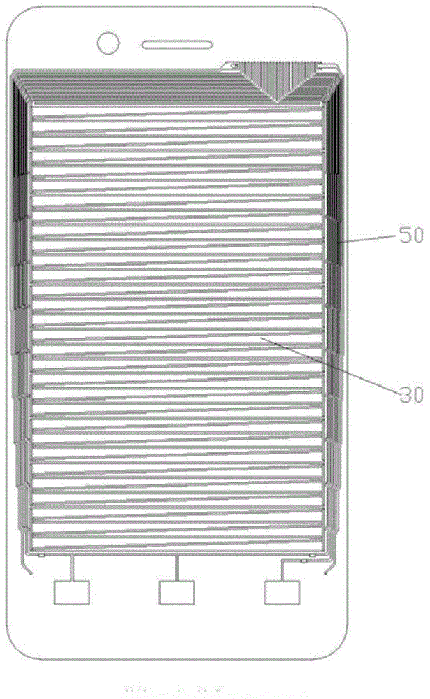
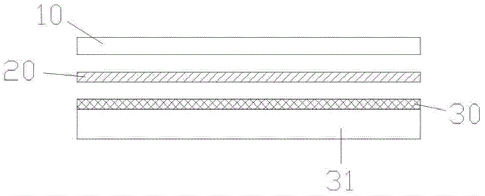
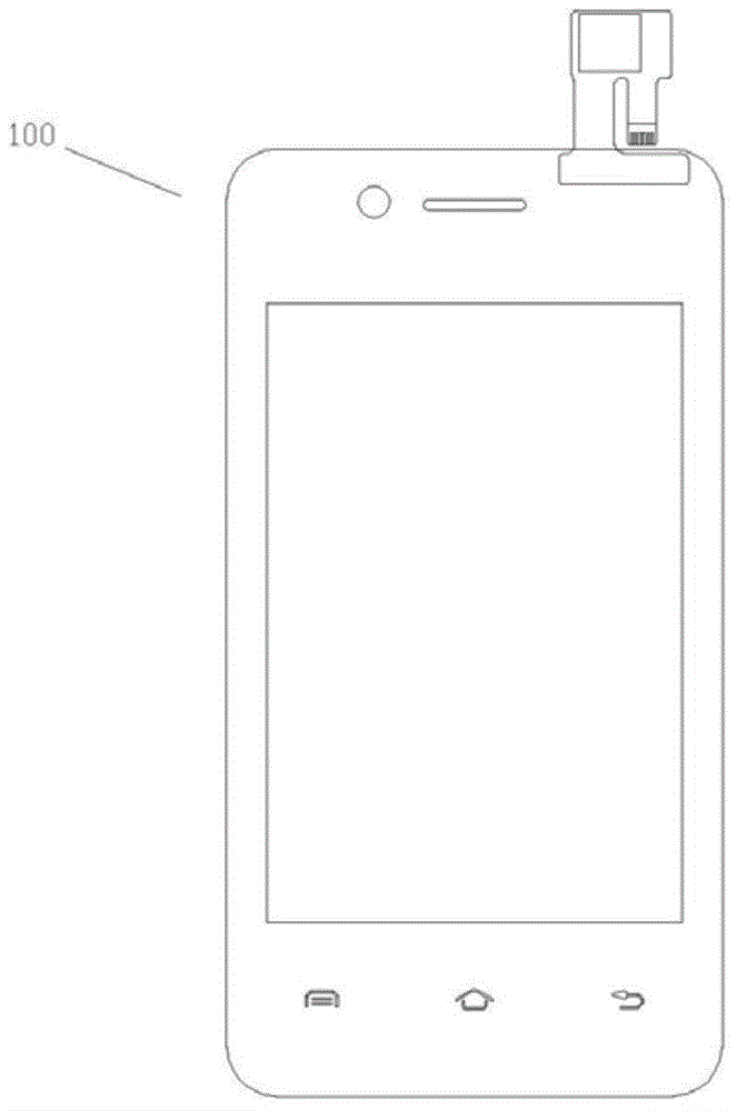
[0076] Such as Figures 1 to 14 As shown, a graphene capacitive touch screen 100 includes a cover layer 10, an OCA optical adhesive layer 20 and a graphene transparent conductive film layer 30, wherein the OCA optical adhesive layer 20 is arranged between the cover layer 10 and the Between the graphene transparent conductive film layers 30, the cover layer 10 is made of PC material.

[0077] A circuit layer 40 is also arranged on the lower surface of the graphene transparent conductive film layer 30 .

[0078] An electrode layer 50 is arranged around the circuit layer 40 , and the electrode layer 50 is printed with silver paste material. The electrode layer 50 is used to lead out the circuit layer 40 .

[0079] During work, a low-voltage AC electric field is formed in the graphene transparent conductive film layer 30, and when the user's finger touches the surface of the graphene capacitive touch screen, a coupling capacitance will be formed between the finger and the graphen...


PUM


Abstract

The invention relates to a graphene capacitance touch screen and a manufacturing method thereof. The touch screen is characterized by comprising a cover plate layer, an OCA optical clear adhesive layer and a graphene transparent conductive film layer, wherein a circuit layer is arranged on the lower surface of the graphene transparent conductive film layer, and an electrode layer is arranged on the periphery of the circuit layer, and is used for leading out the circuit layer. When the touch screen works, a low-voltage alternating-current electric field is formed in the graphene transparent conductive film layer, when a user finger touches the surface of the graphene capacitance touch screen, a coupling capacitor is formed between the finger and the graphene transparent conductive film layer, and a certain amount of electric charge is transferred to the human body at that time, and electric charge is supplied from four corners of the graphene capacitance touch screen to restore the electric charge loss, and the distance of the electric charge amount supplied from each direction and the touching point is proportional, so that the location of the touching point can be calculated.

Description

technical field [0001] The invention relates to a capacitive touch screen and a manufacturing method thereof, in particular to a structure and a processing method formulated for the composition of graphene. Background technique [0002] As we all know, transparent conductive film is an important optoelectronic material, which is widely used in optoelectronic fields such as touch screens, liquid crystal displays, organic light-emitting diode displays (OLEDs), and solar cells. Graphene is a new type of carbon material discovered by Professor AK Geim of the University of Manchester in 2004. It is a two-dimensional honeycomb structure composed of a single layer of carbon atoms. Since its discovery, graphene has quickly attracted widespread attention from academia and business circles, and is currently one of the most eye-catching new materials. The carriers in graphene have zero effective mass and behave similar to photons. These characteristics make graphene exhibit unusual ha...

Claims


Application Information

Patent Timeline
Patent Type & Authority Applications(China)
IPC IPC(8): G06F3/044
Inventor 凌桦光孟磊马来鹏任文才成会明
Owner 深圳市航泰光电有限公司
Learn More