

Local doping method for solar cells
A solar cell and local technology, applied in the field of solar cells, can solve the problems of increasing process steps and costs, and achieve the effect of reducing process cost and process complexity
- Summary
- Abstract
- Description
- Claims
- Application Information
AI Technical Summary
Problems solved by technology
Method used
Image

Examples
Embodiment Construction
[0023] In order to make the content of the present invention more clearly understood, the present invention will be further described in detail below based on specific embodiments and in conjunction with the accompanying drawings.
[0024] A local doping method for solar cells, the steps of the method are as follows:
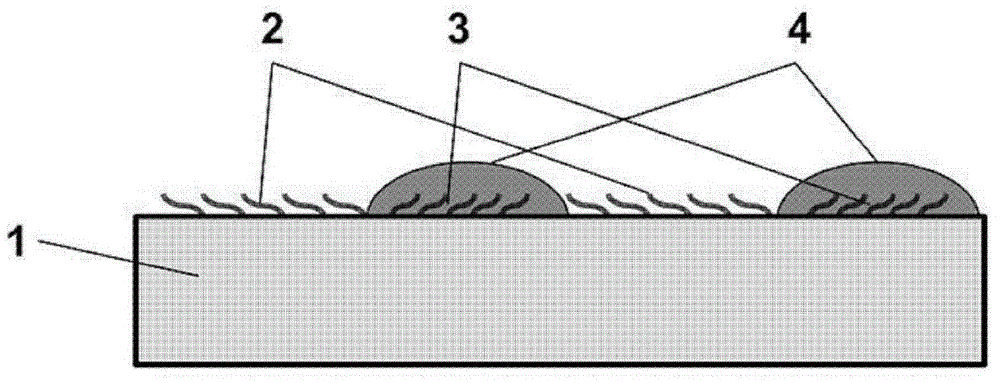
[0025] a) According to the structure of the solar cell, modify the molecular film of the corresponding pattern on the surface of the substrate 1 of the solar cell, such as figure 1 shown; wherein, there are hydrophilic groups and hydrophobic groups in the molecular membrane; the hydrophilic groups are -OH or -COH or -COOH or -NH 2 ; The hydrophobic group is -S or -Cl or -F or -NO 2 .
[0026] b) setting a solution containing the dopant source 4 on the substrate 1 processed in step a), and having a polar solvent in the solution, so that the dopant source 4 is distributed on the corresponding pattern;
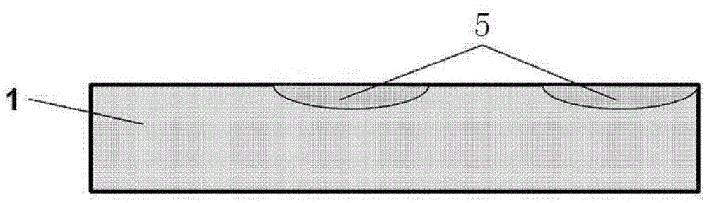
[0027] c) The volatile solution can be volatilized natural...
PUM
 Abstract
Description
Claims
Application Information