Method for manufacturing fin field effect transistor

A technology of fin field effect and manufacturing method, which is applied in semiconductor/solid-state device manufacturing, semiconductor devices, electrical components, etc., can solve problems such as unfavorable oxide filling, reducing device stability, etc., so as to improve device performance and increase filling process. effect of windows, improved process efficiency and etch accuracy

Inactive Publication Date: 2014-09-10
SHANGHAI HUALI MICROELECTRONICS CORP
View PDF4 Cites 14 Cited by
  • Summary
  • Abstract
  • Description
  • Claims
  • Application Information

AI Technical Summary

Problems solved by technology

[0006] Since part of the vertical fins on the fin structure 12 is not conducive to the filling of the oxide, there are gaps 15 in the shallow trench isolation 11, which obviously will greatly reduce the stability of the device.

Method used


Image

  • Method for manufacturing fin field effect transistor
  • Method for manufacturing fin field effect transistor
  • Method for manufacturing fin field effect transistor

Examples


Embodiment Construction

[0029] In order to make the purpose and features of the present invention more obvious and easy to understand, the following will further describe the specific embodiments of the present invention in conjunction with the accompanying drawings. However, the present invention can be realized in different forms, and should not be considered as being limited to the described embodiments .

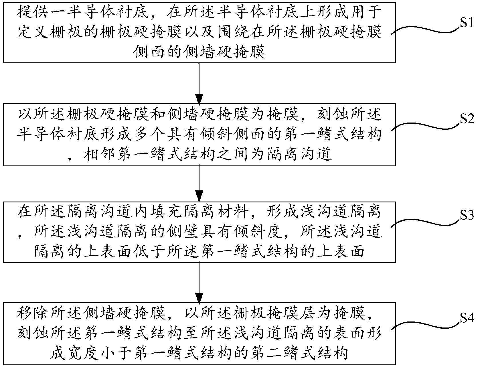
[0030] Please refer to figure 2 , the present embodiment provides a method for manufacturing a fin field effect transistor, including:

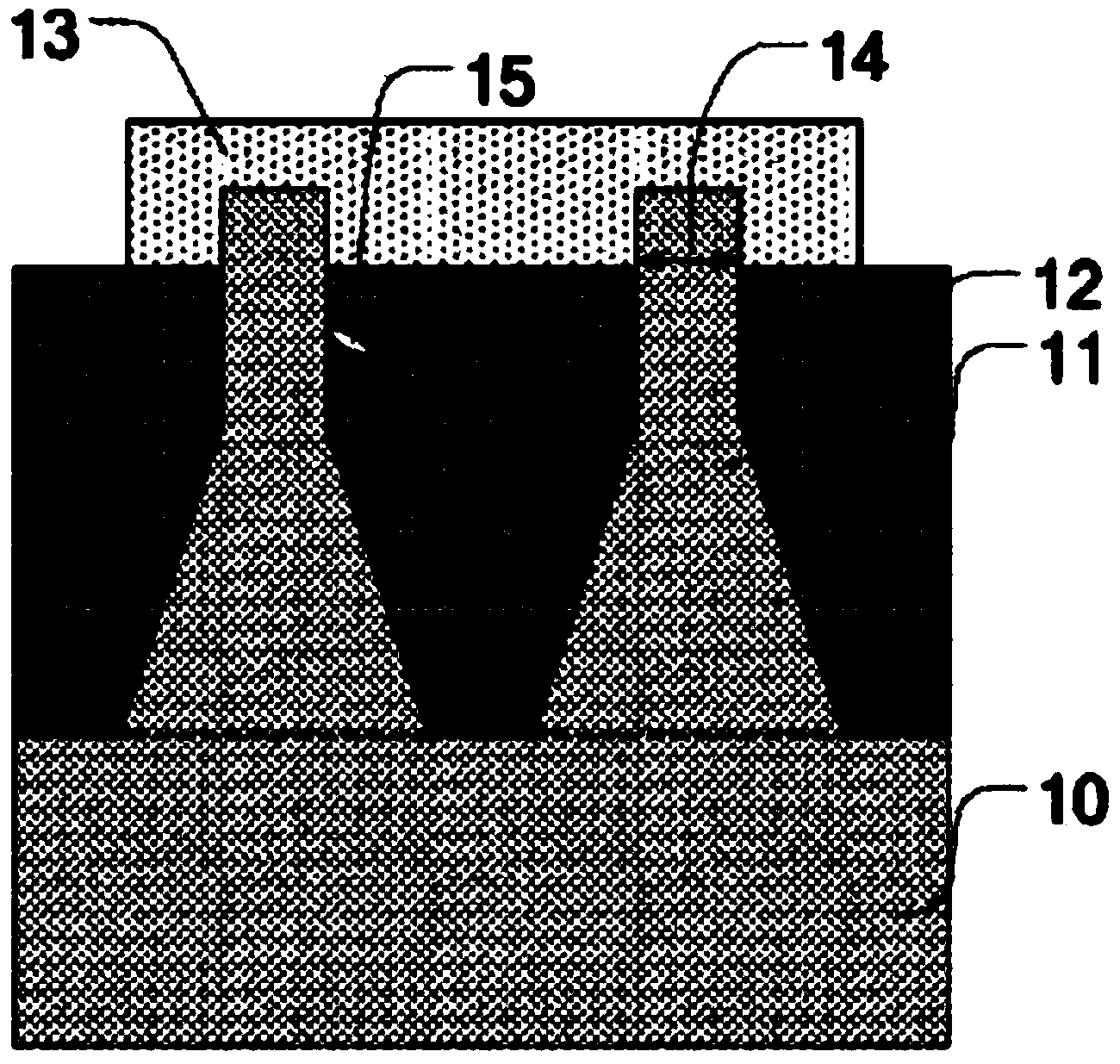
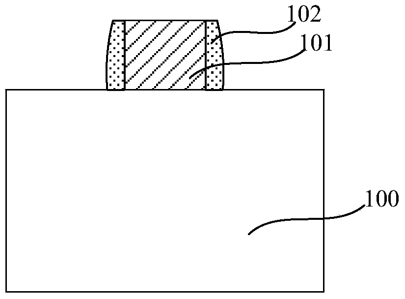
[0031] S1, providing a semiconductor substrate, forming a gate hard mask for defining a gate and a sidewall hard mask surrounding the sides of the gate hard mask on the semiconductor substrate;

[0032] S2, using the gate hard mask and the sidewall hard mask as a mask, etch the semiconductor substrate to form a plurality of first fin structures with inclined sides, and between adjacent first fin structures is isolation trench;

[0033] S3, filling the isol...


PUM


Abstract

The invention provides a method for manufacturing a fin field effect transistor. The method includes forming a grid hard mask used for positioning a grid and a side wall hard mask surrounding the side face of the grid hard mask on a semiconductor substrate; by utilizing the side wall hard mask as a self-aligning hard mask, enabling the semiconductor substrate to form first fin structures with inclined side faces, forming shallow groove isolators among the first fin structures , removing the side wall hard mask, performing second-time etching, and finally acquiring the fin field effect transistor where the upper portion and the lower portion are different in width. The side faces of the fin structures are inclined when the shallow groove isolators are formed in a filling oxidation layer, so that filling process windows are increased, filling gaps are reduced, and device performance is improved.

Description

technical field [0001] The invention relates to the field of semiconductor manufacturing, in particular to a method for manufacturing a fin field effect transistor. Background technique [0002] In order to keep up with the pace of Moore's Law, people have to continue to shrink the feature size of MOSFET transistors. Doing so can bring benefits such as increasing chip density and improving the switching speed of MOSFETs. As the feature size (CD, Critical Dimension) of the device further decreases, the channel length of the device is shortened, and the distance between the drain and the source is also shortened, so that the control ability of the gate to the channel becomes worse, and the gate voltage It is more and more difficult to pinch off the channel, so that the phenomenon of subthreshold leakage (Subthreshold leakage), the so-called short-channel effect (SCE: short-channel effects) is more likely to occur. [0003] For this reason, the planar CMOS transistor is gradu...

Claims


Application Information

Patent Timeline
Patent Type & Authority Applications(China)
IPC IPC(8): H01L21/336
CPCH01L29/66795H01L29/1033
Inventor 鲍宇
Owner SHANGHAI HUALI MICROELECTRONICS CORP
Why Eureka
Try Eureka