Lead-free solder capable of achieving evenly organized soldering spots and soldering method thereof

A technology of lead-free solder and welding method, applied in the direction of welding medium, welding equipment, welding/cutting medium/material, etc., can solve the problem that the solder does not meet the development needs of welding technology, and achieve the effect of good application prospects

Active Publication Date: 2014-09-17
HOERSON ELECTRONICS TECH +1
View PDF5 Cites 8 Cited by
  • Summary
  • Abstract
  • Description
  • Claims
  • Application Information

AI Technical Summary

Problems solved by technology

[0004] In view of the above-mentioned deficiencies in the prior art, the purpose of the present invention is to provide a lead-free solder and its soldering method that can form a uniform solder joint, aiming to solve the problem that the current solder does not meet the development needs of the soldering process

Method used


Image

  • Lead-free solder capable of achieving evenly organized soldering spots and soldering method thereof
  • Lead-free solder capable of achieving evenly organized soldering spots and soldering method thereof
  • Lead-free solder capable of achieving evenly organized soldering spots and soldering method thereof

Examples


Embodiment 1

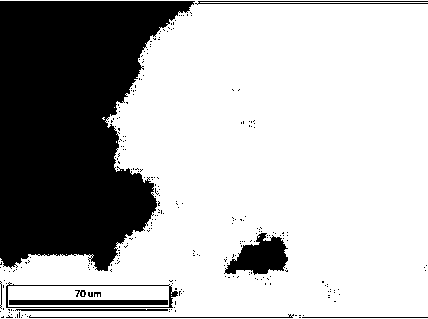
[0032] Take 60 grams of Sn58Bi powder with a particle size range of 25 μm-45 μm and 30 grams of Sn1.0Ag0.5Cu powder and mix thoroughly, and then add 10 grams of rosin flux to make solder paste. The solder paste is coated on the electronic components, and soldered at 180°C. image 3 Shown is the overall organizational structure of its solder joints, Figure 4 Shown is its crystal orientation map (one grayscale represents one crystal orientation), from image 3 and Figure 4 It can be seen that the solder joint grain obtained with the composite solder paste of embodiment 1 is relatively figure 2 For Comparative Example 1 shown, the grains of the solder joints are fine.

Embodiment 2

[0034] Take 55 grams of Sn57Bi1Ag powder with a particle size range of 20 μm-38 μm and 35 grams of Sn3.0Ag0.5Cu powder and mix thoroughly, and then add 10 grams of rosin flux to make solder paste. Coat the solder paste on the electronic components and perform soldering under the condition of 180°C. Figure 5 Shown is the overall organizational structure of the solder joints, Figure 6 Shown is its crystal orientation map (one grayscale represents one crystal orientation), from Figure 5 and Figure 6 It can be seen that the solder joint grain obtained with the composite solder paste of embodiment 2 is relatively figure 2 For Comparative Example 1 shown, the grains of the solder joints are fine.

Embodiment 3

[0035]Example 3: Take 40 grams of Sn57.6Bi0.4Ag powder with a particle size range of 25 μm-45 μm and 50 grams of Sn3.0Ag0.5Cu powder and mix thoroughly, and then add 10 grams of rosin flux to prepare solder paste. Coat the solder paste on the electronic components and perform soldering under the condition of 180°C.


PUM

PropertyMeasurementUnit
melting pointaaaaaaaaaa
particle diameteraaaaaaaaaa

Abstract

The invention discloses a lead-free solder capable of achieving evenly organized soldering spots and a soldering method of the lead-free solder. The lead-free solder is formed by mixing low-temperature solder powder and high-temperature solder powder according to the mass ratio ranging from 3:1 to 1:3 and adding soldering flux or soldering paste into the mixture, wherein the melting temperature of the low-temperature solder powder ranges from 110 DEG C to 150 DEG C, and the melting temperature of the high-temperature solder powder ranges from 210 DEG C to 230 DEG C. The lead-free solder is free of lead and solves the problem that traditional lead-free solder is over high in melting temperature currently, low-temperature soldering of the lead-free solder is achieved, and therefore the lead-free solder can be applied to soldering of materials of electronic components developed on the basis of Sn-Pb eutectic solder and can effectively replace the Sn-Pb eutectic solder, and the lead-free solder has good application prospects in the field of electronic packaging.

Description

technical field [0001] The invention relates to the field of soldering materials, in particular to a lead-free solder capable of forming uniform solder joints and a soldering method thereof. Background technique [0002] With the in-depth understanding of the toxicity of Pb in the society and the implementation of the EU WEEE / ROHS Act on July 1, 2006, it is the general trend to replace the traditional Sn-Pb solder with lead-free solder. At present, lead-free alloys such as Sn-Ag, Sn-Cu, and Sn-Ag-Cu have been widely used in the field of electronic packaging. The melting point of these lead-free solder alloys is generally 217-227°C, which is much higher than the melting point of the traditional Sn-Pb eutectic solder (183°C). Therefore, the use of lead-free solder has brought new problems after solving environmental problems. . First of all, the increased soldering temperature is not conducive to energy saving and emission reduction; secondly, since the current electronic pa...

Claims


Application Information

Patent Timeline
Patent Type & Authority Applications(China)
IPC IPC(8): B23K35/24B23K1/00
CPCB23K1/0016B23K35/262B23K2101/36
Inventor 马鑫任晓敏
Owner HOERSON ELECTRONICS TECH
Why Eureka
Try Eureka