Method for detecting depth of etched groove through current change

A technology of current change and etching grooves, which is applied in electromagnetic measuring devices, electric/magnetic depth measurement, and processes for producing decorative surface effects, etc. Monitor, avoid damage, and accurately grasp the effect

Inactive Publication Date: 2014-09-17
PEKING UNIV +1
View PDF3 Cites 7 Cited by
  • Summary
  • Abstract
  • Description
  • Claims
  • Application Information

AI Technical Summary

Problems solved by technology

However, this method will obviously cause a deviation between the etching completion result and the design result.

Method used


Image

  • Method for detecting depth of etched groove through current change
  • Method for detecting depth of etched groove through current change
  • Method for detecting depth of etched groove through current change

Examples


Embodiment 1

[0044] The specific implementation process of the method for detecting the depth of the etching groove by using the current change in this embodiment is as follows: Figure 1(a) ~ Figure 1(g) As shown, the specific description is as follows:

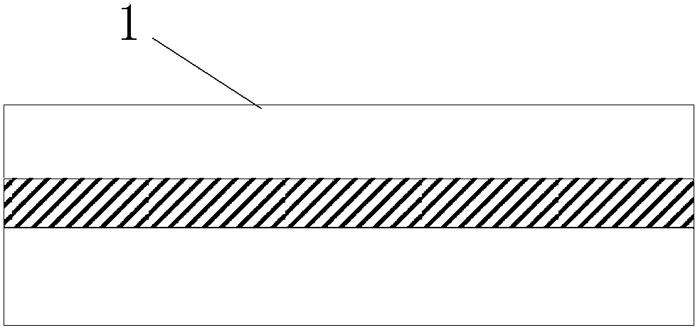
[0045] 1. Preparation: SOI substrate 1 is used as the substrate of the chip, as shown in FIG. 1( a ).

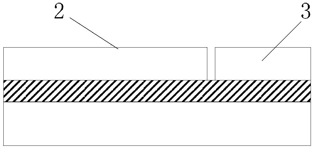
[0046] 2. Use MEMS process photolithography on the substrate to define the detection area 3, and use the etching process to isolate the detection area 3 and the functional area 2, including: As shown in Figure 1(b).

[0047] The etching depth value is the thickness of the silicon layer on the front side of the SOI silicon wafer, and the front side silicon layer is etched through the etching process to realize the electrical insulation between the detection area 3 and the functional area 2 .

[0048] That is to say, in the present invention, the functional area and the detection area of ​​the device are isolated by the buried oxide l...


PUM


Abstract

The invention discloses a method for detecting the depth of an etched groove through the current change. A special detection region is designed, so that the depth of the etched groove is reflected in real time. The detection region is prepared through the MEMS processing technique and signals are read through a current meter. According to the method, a function region and the detection region are well isolated electrically through an SOI silicon wafer and the MEMS processing technique and the function region is prevented from being damaged through detection current. Meanwhile, through pattern transfer, etched windows of the function region are copied in the detection region and it is guaranteed that the etching conditions of the detection region tend to be identical to those of the function region. Strict electricity modeling calculation is conducted on the deep groove structure of the detection region, the relation between the etching depth and current signals is acquired, and on the basis, the depth of the etched groove is monitored in real time through detection of the current meter.

Description

technical field [0001] The invention belongs to the field of micro-electro-mechanical system (MEMS) processing technology. By designing a detection area on a silicon chip that needs to be etched with a deep groove structure, using a tiny current meter to measure the magnitude of the current passing through the detection structure, and using this as a standard, Determine the instant depth of etching on the silicon wafer to achieve the purpose of observing the depth of the etching groove at all times. Background technique [0002] Micro-Electro-Mechanical Systems (MEMS) is an important direction for the development and application of microelectronics technology, and etching technology is an important means to realize material removal, image transfer and core structure preparation in MEMS processing technology. The current etching technology is mainly divided into wet etching and dry etching. Since it is difficult to obtain a high aspect ratio by wet etching, dry etching techno...

Claims


Application Information

Patent Timeline
Patent Type & Authority Applications(China)
IPC IPC(8): G01B7/26B81C1/00
Inventor 张立何军张大成黄贤赵丹淇王玮杨芳田大宇刘鹏李婷罗葵
Owner PEKING UNIV
Why Eureka
Try Eureka