Chip-stacking encapsulation structure and electronic equipment

A technology of chip stacking and packaging structure, applied in the field of electronics, can solve problems such as difficulty in wiring, and achieve the effects of reducing wiring space resources, improving performance, and improving resource utilization.

Active Publication Date: 2014-09-24
HUAWEI TECH CO LTD
View PDF4 Cites 11 Cited by
  • Summary
  • Abstract
  • Description
  • Claims
  • Application Information

AI Technical Summary

Problems solved by technology

[0007] Embodiments of the present invention provide a chip stack package structure and electronic equipment, which solves the problem of difficult routing caused by opening holes on the periphery of the package in the prior art

Method used


Image

  • Chip-stacking encapsulation structure and electronic equipment
  • Chip-stacking encapsulation structure and electronic equipment
  • Chip-stacking encapsulation structure and electronic equipment

Examples


Embodiment 1

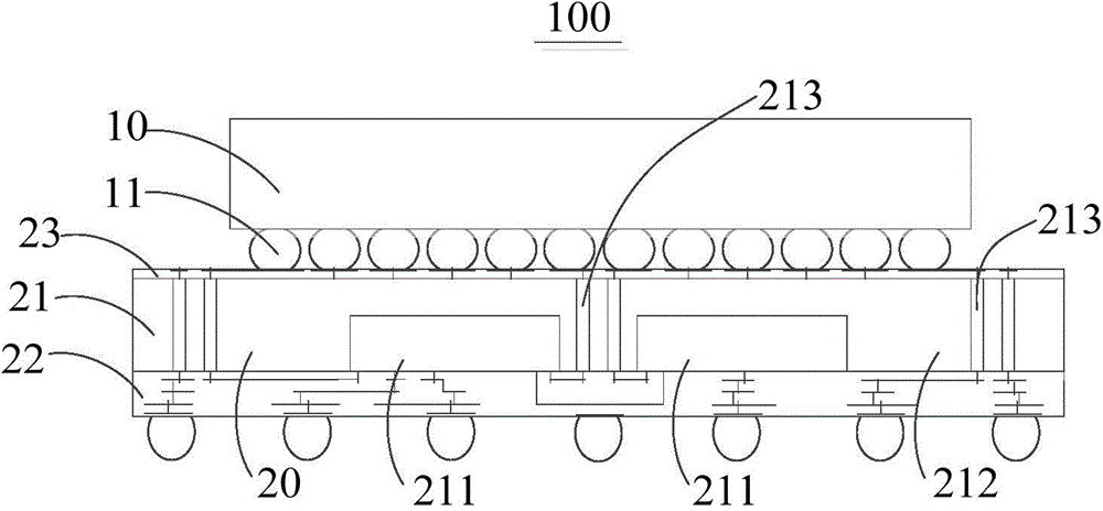
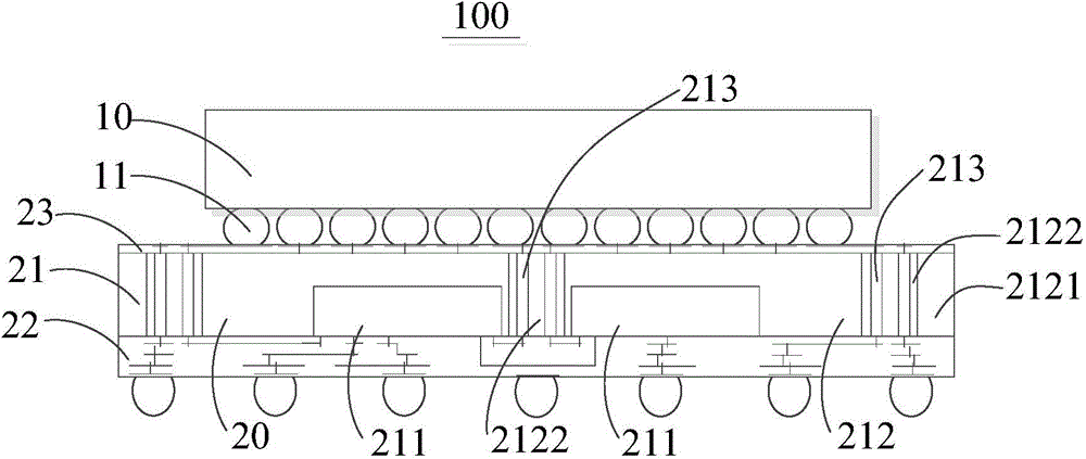
[0029] Such as figure 1 As shown, it is a schematic structural diagram of a chip stack package structure 100 provided by a preferred embodiment of the present application. The chip stack package structure 100 includes a first chip 10 and a second chip 20 .

[0030] The first chip 10 may be a memory chip (Memory), a silicon grain (Silicon Die), a flip-chip package structure (Flip Chip Package), a passive device (Passive Device), etc., or may be an integrated single or multiple chip Die fan-out wafer level packaging. Solder balls 11 are disposed on the first chip 10 , and the first chip 10 can be electrically connected with other electronic components through the solder balls 11 . The solder ball 11 may be a solder ball (Solder Ball), a solder bump (Solder Bump) or a copper pillar (Cu Pillar).

[0031] see also figure 2 , the second chip 20 and the first chip 10 are stacked and fixed to each other. The structure of the second chip 20 is the same as that of the first chip 1...

Embodiment 2

[0047] Based on the same inventive concept, the present application also provides an electronic device. Such as Figure 5 As shown, is a schematic structural diagram of the electronic device 200 of the present application. The electronic device 200 includes a circuit board 210 and a chip stack package structure 220 disposed on the circuit board. The structure and function of the chip stack package structure 220 are the same as those of the chip stack package structure 100 in the first embodiment, and will not be repeated here. The second chip 20 of the chip stack package structure 220 is located between the first chip 10 and the circuit board 210 .

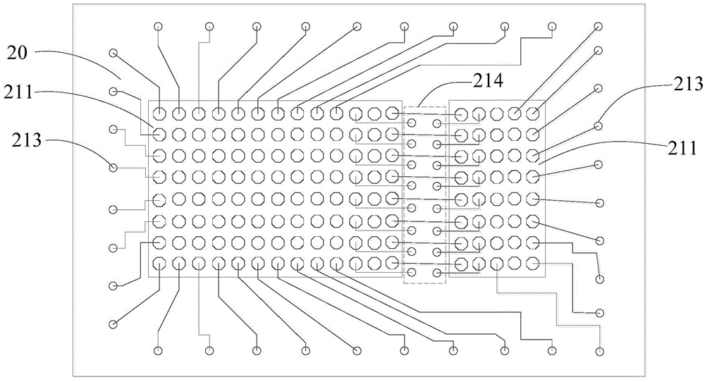
[0048] The above-mentioned electronic device 200 adopts the chip stacking package structure 220, and adds a through hole 213 between at least two dies 211 of the second chip 20, so that the fan-out input and output lines on the die 211 can be directly passed through. The through hole 213 around the crystal grain 211 is electric...


PUM


Abstract

The embodiment of the invention discloses a chip-stacking encapsulation structure and electronic equipment. The chip-stacking encapsulation structure comprises a first chip and a second chip, wherein the second chip and the first chip are arranged in a stacking manner, the second chip comprises an encapsulation layer and a first wiring layer, the encapsulation layer comprises at least two crystalline grains and a fixing portion used for fixing the at least two crystalline grains, a plurality of through holes are opened in the fixing portion, a part of the through holes of the plurality of through holes is formed in the peripheries of the at least two crystalline grains, and the other part of the through holes of the plurality of through holes is formed between the at least two crystalline grains; the first wiring layer is electrically connected with the at least two crystalline grains; the encapsulation layer is located between the first wiring layer and the first chip, conductive materials are arranged in the plurality of through holes, and the first wiring layer and the first chip are electrically connected by the conductive materials, thus the first chip can be electrically connected with at least one of the at least two crystalline grains.

Description

technical field [0001] The invention relates to the field of electronic technology, in particular to a chip stack packaging structure and electronic equipment. Background technique [0002] With the development of the semiconductor industry, the requirements for the integration and miniaturization of semiconductor chips are getting higher and higher. In order to meet the requirements of integration and miniaturization of semiconductor chips, packaging technology has also been improved continuously, and various stacked packaging technologies have been developed one after another, and are becoming more and more important. [0003] Common packaging technologies include wire bonding (Wire bonding) packaging, flip-chip bonding (Flip-chip bonding) packaging and the resulting stacked packaging (Package On Package), through silicon via (Through Silicon Via, TSV) packaging, Fan Out Wafer Level Package (FOWLP), etc. [0004] The upper chip and the lower chip of the existing fan-out ...

Claims


Application Information

Patent Timeline
IPC IPC(8): H01L23/538
CPCH01L2224/16225H01L23/49816H01L23/5384H01L23/5389H01L25/105H01L2224/04105H01L2224/12105H01L2224/131H01L2224/13147H01L2224/16227H01L2224/24137H01L2224/73204H01L2225/1035H01L2225/1041H01L2225/1058H01L2924/10253H01L2924/1434H01L2924/15311H01L2924/014H01L23/481H01L23/528H01L25/0652H01L2225/06548H01L2225/06555H01L2225/06572
Inventor 符会利张晓东
Owner HUAWEI TECH CO LTD
Why Eureka
Try Eureka