Array substrate, manufacturing method thereof, and display device

The technology of an array substrate and a manufacturing method, which is applied in the field of display devices, can solve problems such as poor connections, and achieve the effects of reducing the probability of disconnection, good display images, and reliable electrical connections

Active Publication Date: 2017-01-25
BOE TECH GRP CO LTD +1
View PDF4 Cites 0 Cited by
  • Summary
  • Abstract
  • Description
  • Claims
  • Application Information

AI Technical Summary

Problems solved by technology

Since the passivation layer 50 and the etch stop layer 31 have a relatively large thickness, when forming the connection portion 70, a gap is easily generated on the sidewall of the via hole 60, resulting in a gap between the common electrode line 20 and the common electrode 10. poor connectivity

Method used


Image

  • Array substrate, manufacturing method thereof, and display device
  • Array substrate, manufacturing method thereof, and display device
  • Array substrate, manufacturing method thereof, and display device

Examples


Embodiment Construction

[0052] Specific embodiments of the present invention will be described in detail below in conjunction with the accompanying drawings. It should be understood that the specific embodiments described here are only used to illustrate and explain the present invention, and are not intended to limit the present invention.

[0053] It should be understood that the orientation words "up and down" used in the specification all refer to the "up and down" directions in the drawings.

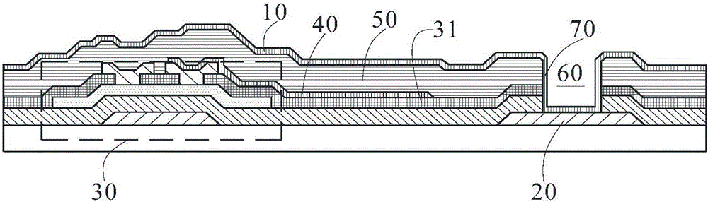
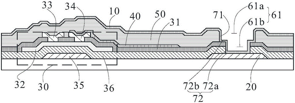
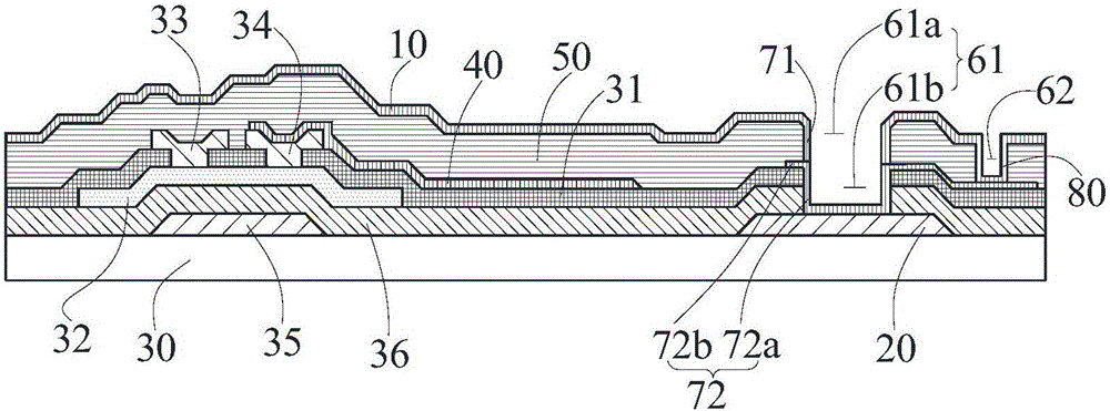
[0054] Such as figure 2 and image 3As shown in, as one aspect of the present invention, an array substrate, the array substrate includes a common electrode line 20, a thin film transistor 30, a common electrode 10, the common electrode line 20 is located below the active layer 32 of the thin film transistor 30, and the common electrode A main transition hole 61 is disposed above the wire 20 . Wherein, the common electrode 10 is electrically connected to the common electrode line 20 through a main conn...


PUM


Abstract

The present invention provides an array substrate, the array substrate includes a common electrode line, a thin film transistor, and a common electrode, the common electrode line is located below the active layer of the thin film transistor, and a main transfer hole is arranged above the common electrode line, wherein the common electrode passes through The main connection part at least partially arranged in the main transfer hole is electrically connected to the common electrode line, the main connection part includes an upper main connection part and a lower main connection part, and the lower main connection part includes a main body and is arranged on the main body and faces away from the main The flange extending in the direction of the center of the transfer hole, the lower end of the upper main connection part is connected with the flange, and the upper end of the upper main connection part is connected with the common electrode. The invention also provides a manufacturing method of the array substrate and a display device including the array substrate. In the array substrate provided by the present invention, there is a reliable electrical connection between the common electrode lines and the common electrode lines. Therefore, the display device including the array substrate can display images better.

Description

technical field [0001] The present invention relates to the field of display technology, in particular, to an array substrate, a method for manufacturing the array substrate, and a display device including the array substrate. Background technique [0002] figure 1 Shown in is an array substrate, the array substrate includes a common electrode 10 , a common electrode line 20 , a thin film transistor 30 and a pixel electrode 40 , and the common electrode 10 is electrically connected to the common electrode line 20 . An etching barrier layer 31 and a passivation layer 50 are also provided between the layer where the common electrode 10 is located and the layer where the common electrode line 20 is located. The via hole 60 is provided, and while the common electrode 10 is deposited and formed, a layer of common electrode material is also formed on the side wall and the bottom wall (that is, the upper surface of the common electrode line 20 ) of the via hole 60 . The common el...

Claims


Application Information

Patent Timeline
Patent Type & Authority Patents(China)
IPC IPC(8): H01L27/12H01L21/77G02F1/1333
CPCH01L27/1244G02F1/136227H01L27/1225G02F1/1333H01L27/124H01L27/127H01L29/7869
Inventor 龙跃李凡王杨
Owner BOE TECH GRP CO LTD
Why Eureka
Try Eureka