Method of making liquid crystal display panel
A liquid crystal display panel and liquid crystal layer technology, applied in nonlinear optics, instruments, optics, etc., can solve problems such as poor alignment of liquid crystal molecules, and achieve the effect of solving poor alignment and uniform arrangement
- Summary
- Abstract
- Description
- Claims
- Application Information
AI Technical Summary
Problems solved by technology
Method used
Image
Examples
Embodiment Construction
[0028] The present invention will be described in detail below in conjunction with the accompanying drawings and specific embodiments, but not as a limitation of the present invention.
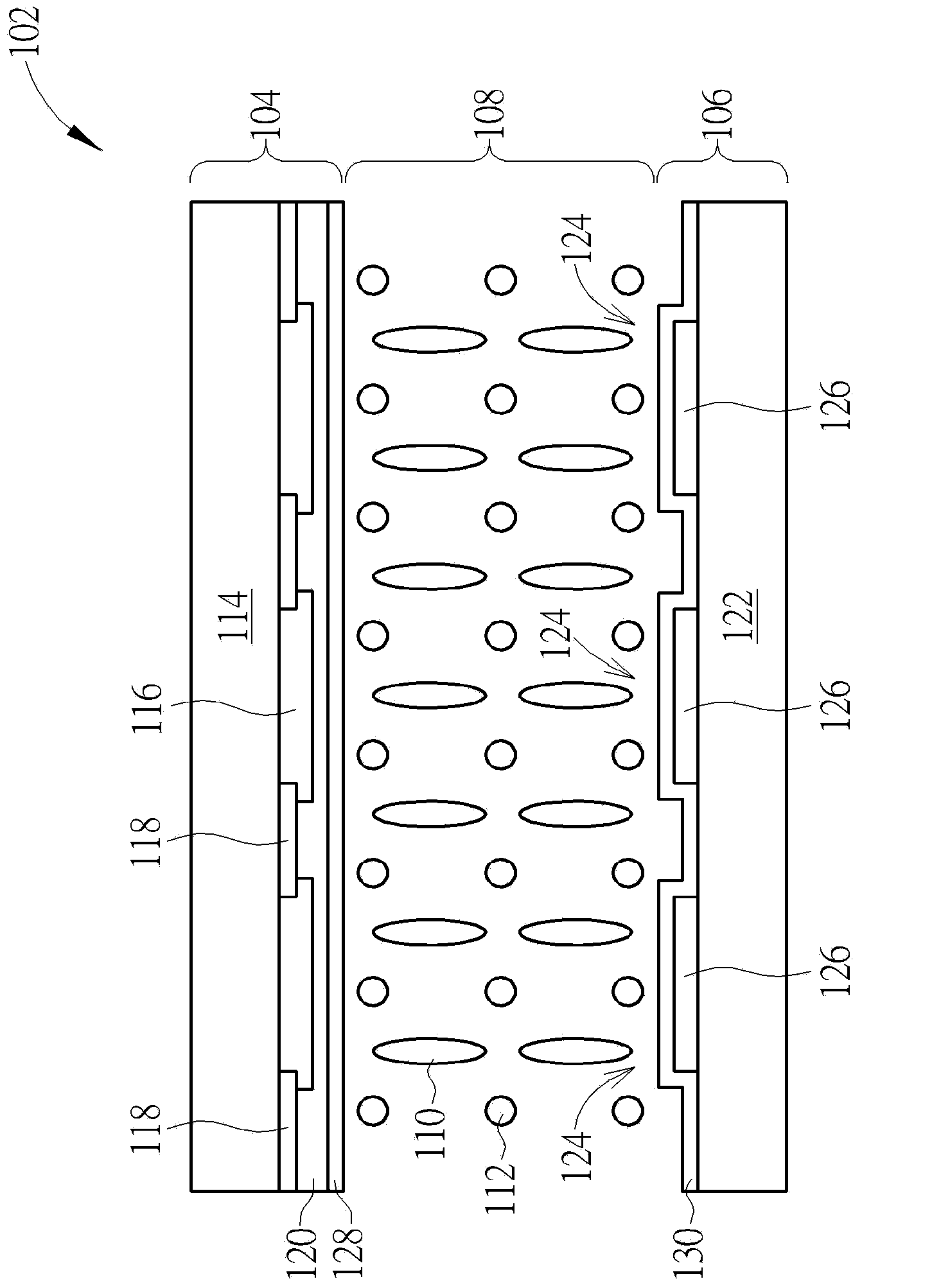
[0029] Please refer to Figure 2 to Figure 7 , Figure 2 to Figure 7 It is a schematic diagram of the method for manufacturing a liquid crystal display panel according to the first embodiment of the present invention, wherein image 3 is a schematic top view of the pixel electrode of the liquid crystal display panel according to the first embodiment of the present invention, and Figure 5 It is a schematic diagram of the relationship between the voltage signal and time in the first embodiment of the present invention. Such as figure 2 and image 3 As shown, firstly, a liquid crystal display panel semi-finished product 102 is provided. At this point, the liquid crystal display panel semi-finished product 102 already includes the upper substrate 104 , the lower substrate 106 and the liquid...
PUM
 Abstract
Description
Claims
Application Information


