Magnetron sputtering device and magnetron sputtering method

A magnetron sputtering and equipment technology, applied in the field of microelectronics processing, can solve the problems of increasing difficulty, unsolved film uniformity, adverse effects, etc., and achieve the effect of improving process quality, film uniformity and deposition rate

Active Publication Date: 2014-10-22
BEIJING NAURA MICROELECTRONICS EQUIP CO LTD
View PDF6 Cites 10 Cited by
  • Summary
  • Abstract
  • Description
  • Claims
  • Application Information

AI Technical Summary

Problems solved by technology

But this will have the following problems again, that is, because the deposition time needs to be adjusted continuously according to the real-time change of the target-substrate spacing, this not onl

Method used


Image

  • Magnetron sputtering device and magnetron sputtering method
  • Magnetron sputtering device and magnetron sputtering method
  • Magnetron sputtering device and magnetron sputtering method

Examples


Example Embodiment

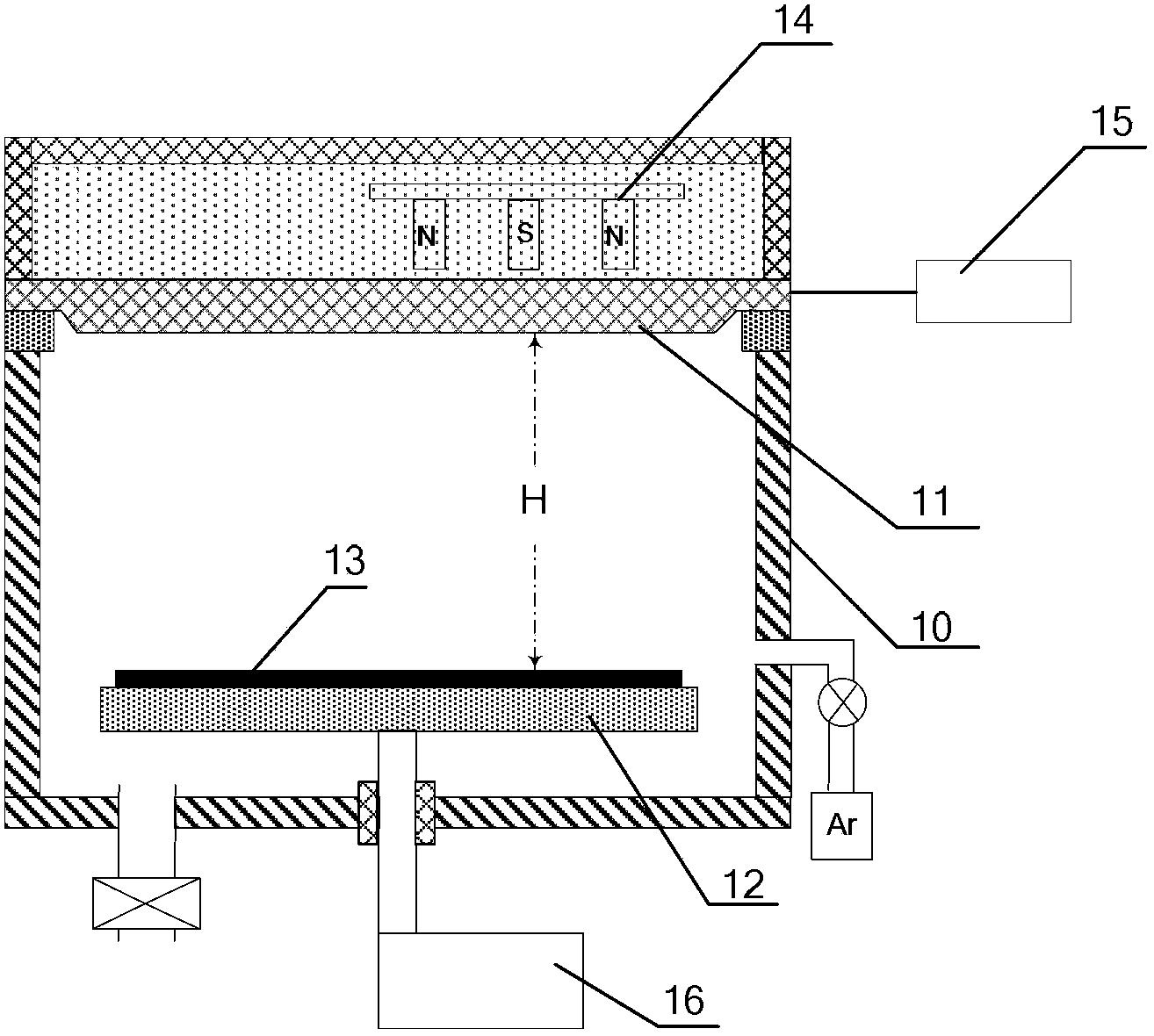
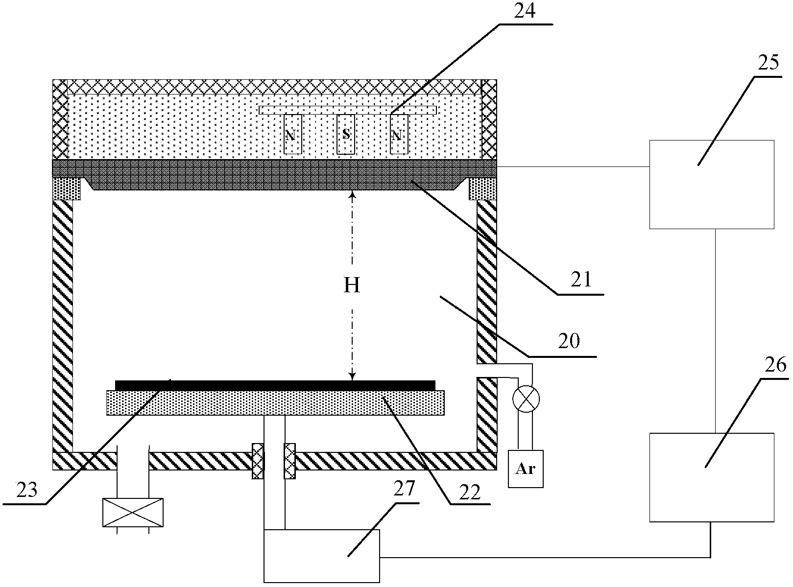
[0040] In order to enable those skilled in the art to better understand the technical solution of the present invention, the magnetron sputtering equipment and the magnetron sputtering method provided by the present invention will be described in detail below in conjunction with the accompanying drawings.

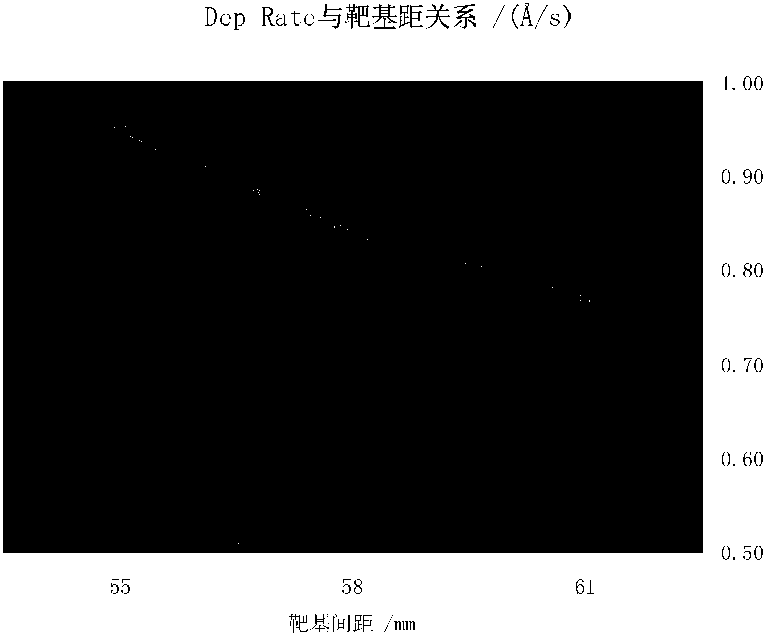
[0041] image 3 Schematic diagram of the structure of the magnetron sputtering equipment provided by the present invention. Figure 4 The schematic block diagram of the magnetron sputtering equipment provided by the present invention. Please also refer to image 3 and Figure 4 , the magnetron sputtering device includes a reaction chamber 20 , a sputtering power supply 25 , a driving source 27 and a control unit 26 . Wherein, the top of reaction chamber 20 is provided with target material 21, and sputtering power supply 25 is electrically connected with target material 21, and in magnetron sputtering process, sputtering power supply 25 outputs sputtering power to target ...


PUM


Abstract

The present invention provides a magnetron sputtering device and a magnetron sputtering method. The magnetron sputtering device comprises a reaction chamber, a sputtering power supply and a driving source, a target is arranged at the top of the reaction chamber, and the sputtering power supply is electrically connected with the target, and is used to output a sputtering power to the target during the magnetron sputtering process. A pedestal is arranged in the reaction chamber, is located below the target, and is used to bear a processed workpiece. The driving source is used to drive the pedestal to rise or drop. Moreover, the magnetron sputtering device also comprises a control unit used for controlling the driving source to drive the pedestal to rise during the magnetron sputtering process, so that the spacing between the target and the pedestal is always kept at a predetermined value and does not change. The magnetron sputtering device provided by the present invention uses the control unit to control the driving source to drive the pedestal to rise during the magnetron sputtering process, so that the spacing between the target and the pedestal is always kept at the predetermined value, does not change, and is always kept at an optimal value, and accordingly, the thin film uniformity and deposition rate can be improved.

Description

technical field [0001] The invention relates to the technical field of microelectronic processing, in particular to a magnetron sputtering device and a magnetron sputtering method. Background technique [0002] In the microelectronics industry, magnetron sputtering technology is one of the important means of producing integrated circuits, liquid crystal displays, thin-film solar cells and LEDs, and plays a great role in industrial production and scientific fields. In recent years, the market's growing demand for high-quality products has prompted companies to continuously improve magnetron sputtering equipment. [0003] figure 1 It is a structural schematic diagram of an existing magnetron sputtering device. like figure 1 As shown, the magnetron sputtering equipment includes a reaction chamber 10 , a magnetron 14 and a sputtering power supply 15 . Wherein, the top of reaction chamber 10 is provided with target material 11, and sputtering power source 15 is electrically c...

Claims


Application Information

Patent Timeline
IPC IPC(8): H01J37/34C23C14/35
Inventor 文莉辉
Owner BEIJING NAURA MICROELECTRONICS EQUIP CO LTD
Why Eureka
Try Eureka