Heating chamber and semiconductor processing equipment

A technology for heating chambers and chambers, applied in metal material coating process, ion implantation plating, coating, etc., can solve the problems of real-time acquisition of wafer temperature, heating reliability, low process efficiency, etc., to improve heating accuracy and temperature uniformity, improve reliability and process quality, and improve process efficiency

Active Publication Date: 2016-03-30
BEIJING NAURA MICROELECTRONICS EQUIP CO LTD
View PDF4 Cites 9 Cited by
  • Summary
  • Abstract
  • Description
  • Claims
  • Application Information

AI Technical Summary

Problems solved by technology

[0005] However, in practical applications, the following technical problems will inevitably exist in the above method: the temperature of the wafer cannot be obtained in real time during the process, so the temperature of the wafer cannot be controlled in real time, which not only causes poor temperature uniformity of the wafer, but also causes heating The reliability and process quality are poor; and it will also cause when the temperature required by the wafer process or the material of the wafer changes, it is necessary to regain the standard output power before the process, resulting in low process efficiency

Method used


Image

  • Heating chamber and semiconductor processing equipment
  • Heating chamber and semiconductor processing equipment
  • Heating chamber and semiconductor processing equipment

Examples


Embodiment Construction

[0026] In order for those skilled in the art to better understand the technical solution of the present invention, the heating chamber and semiconductor processing equipment provided by the present invention will be described in detail below with reference to the accompanying drawings.

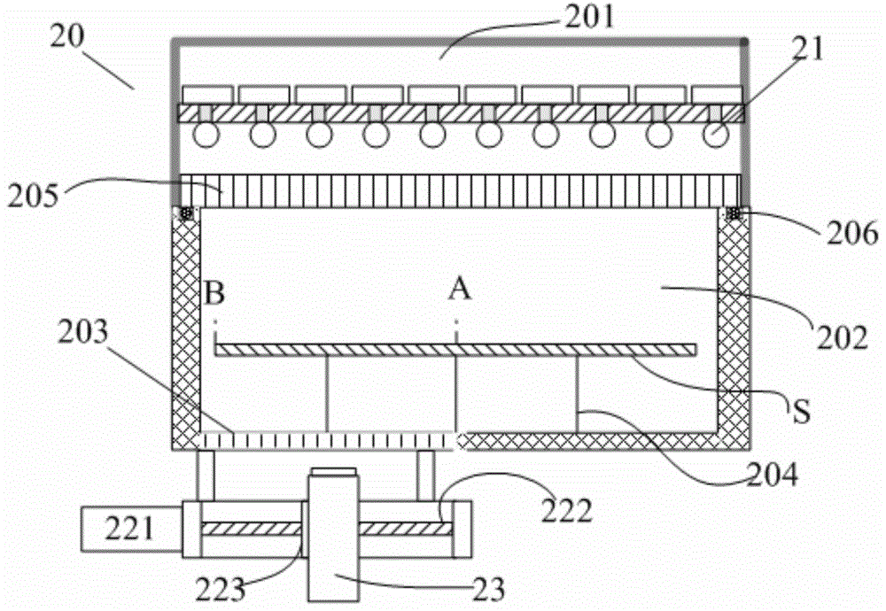
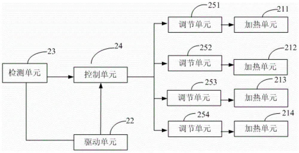
[0027] figure 2 Schematic diagram of the structure of the heating chamber provided by the embodiment of the present invention. image 3 The principle block diagram of the heating chamber provided for the embodiment of the present invention. Please also refer to figure 2 and image 3 , the heating chamber 20 provided in this embodiment is used to realize uniform heating of the wafer, and the heating chamber 20 includes a plurality of heating regions. Multiple concentric regions divided by direction, such as Figure 4 As shown, the heating chamber 20 includes a plurality of concentric heating regions 1-4 divided along the radial direction of the wafer; the heating chamber 20 also includes ...


PUM


Abstract

The present invention relates to a heating chamber and semiconductor processing equipment, the heating chamber comprises a plurality of heating zones, heating units in one-to-one correspondence to the heating zones, a drive unit, a detection unit, a control unit and adjustment units in one-to-one correspondence to the heating units, the drive unit is used for driving the detection unit to move in a plane parallel to a wafer and transmitting a position signal of the detection unit in real time to the control unit, the detection unit is used for detecting in real time the wafer temperature in correspondence to the plurality of heating zones and transmitting the temperature to the control unit, the control unit is used for judging which one of the heating zones, the temperature transmitted by the detection unit belongs to, according to the position signal transmitted by the drive unit and judging whether a bias exists between the temperature and a preset temperature, and if the bias exists between the temperature and the preset temperature, the adjustment unit in correspondence to the heating zone, to which the temperature belongs, is adjusted so as to calibrate the output power of the corresponding heating unit. The heating chamber may improve the heating accuracy and the temperature uniformity and lowers the wafer temperature measurement difficulty.

Description

technical field [0001] The invention belongs to the technical field of microelectronic processing, and in particular relates to a heating chamber and semiconductor processing equipment. Background technique [0002] Physical Vapor Deposition (Physical Vapor Deposition, referred to as PVD) technology is the most widely used thin film manufacturing technology in the semiconductor industry. In the field of integrated circuit manufacturing, PVD technology refers more specifically to magnetron sputtering deposition technology, which is mainly used for the deposition of metal films such as aluminum and copper to form metal contacts and metal interconnections. The PVD process generally includes the following steps: 1) degassing step; 2) pre-cleaning step; 3) copper barrier layer step; 4) copper seed layer step. Among them, the degassing step is mainly to heat the wafer in the degassing chamber to remove the moisture and volatile impurities attached to the surface of the wafer. The...

Claims


Application Information

Patent Timeline
Patent Type & Authority Applications(China)
IPC IPC(8): C23C14/54C23C14/35
Inventor 叶华
Owner BEIJING NAURA MICROELECTRONICS EQUIP CO LTD
Why Eureka
Try Eureka