Double-surface low-parasitic inductance GaN power integrated module

A low parasitic inductance, power integration technology, applied in the direction of circuits, electrical components, electric solid devices, etc., to achieve the effect of reducing area, avoiding oscillation and spikes, and reducing parasitic inductance

Active Publication Date: 2014-10-22
XI AN JIAOTONG UNIV
View PDF4 Cites 29 Cited by
  • Summary
  • Abstract
  • Description
  • Claims
  • Application Information

AI Technical Summary

Problems solved by technology

However, the parasitic oscillation phenomenon still exists, and it is necessary to further optimize the layout and wiring methods to reduce the high-frequency power loop inductance

Method used


Image

  • Double-surface low-parasitic inductance GaN power integrated module
  • Double-surface low-parasitic inductance GaN power integrated module
  • Double-surface low-parasitic inductance GaN power integrated module

Examples


Embodiment Construction

[0020] The present invention will be further described below in conjunction with drawings and embodiments.

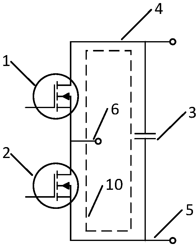
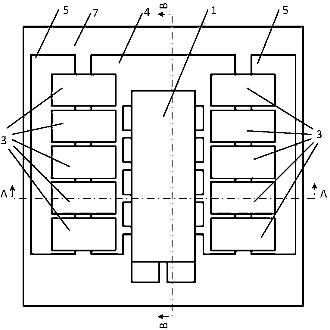
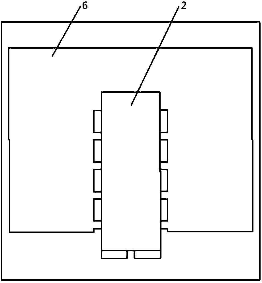
[0021] In the GaN power integrated module of the present invention, the upper bridge arm device 1, the lower bridge arm device 2 and the bus capacitor 3 are sequentially connected to form a high frequency power circuit 10, and the upper bridge arm device 1 and the lower bridge arm device 2 are respectively placed on the substrate 7 (The substrate is a PCB board or LTCC board), the source of the upper bridge arm device 1 and the drain of the lower bridge arm device 2 are placed facing each other, and are directly connected through via holes; the bus capacitor 3 is placed on the upper bridge arm One or both sides of the device 1; all the drains of the upper bridge arm device 1 are connected to one electrode of the bus capacitor 3 on the side close to the bus capacitor, and the other electrode of the bus capacitor 3 is connected to the middle conductive layer 12 through a v...


PUM


Abstract

The invention discloses a double-surface low-parasitic inductance GaN power integrated module. The double-surface low-parasitic inductance GaN power integrated module comprises an upper bridge arm apparatus, a lower bridge arm apparatus and a bus capacitor. The upper bridge arm apparatus and the lower bridge arm apparatus are LGA packaged GaN apparatuses, and the bus capacitor uses chip packaging. One apparatus is arranged at the front surface of a substrate while the other is arranged at the reverse surface of the substrate, and the source electrode of the upper bridge arm apparatus is opposite to the drain electrode of the lower bridge arm apparatus and directly connected with the drain electrode of the lower bridge arm apparatus through holes. The bus capacitor is arranged at two sides of the upper bridge arm apparatus. The arrangement mode of the double-surface low-parasitic inductance GaN power integrated module is capable of effectively reducing the area of a high-frequency power loop and completely uses the crossed structure of LGA packaging drain electrodes and source electrodes to form a plurality of crossed and parallel high-frequency power current loops, and accordingly the parasitic inductance of the high-frequency power loops is greatly lowered, and the over-voltage and oscillation are effectively reduced in the switching process.

Description

technical field [0001] The invention belongs to the technical field of power electronics, and in particular relates to a low parasitic inductance GaN power integrated module with double-sided layout. Background technique [0002] GaN power devices are popular new material devices that have appeared in recent years and have been gradually commercialized. Compared with Si devices, they have superior on-state characteristics and very good switching characteristics, so they have attracted the attention of the industry in a relatively short period of time. , Scholars engaged in applied research have also carried out a lot of research work, applying it to low-voltage, low-power power supply devices such as POL and DC / DC. Studies have shown that replacing Si devices with GaN devices can greatly increase the switching frequency while maintaining good efficiency indicators. Undoubtedly, in low-voltage and low-power applications, GaN devices will be more and more widely used, and wil...

Claims


Application Information

Patent Timeline
Patent Type & Authority Applications(China)
IPC IPC(8): H01L23/31
Inventor 王康平杨旭曾翔君马焕余小玲郭义宣
Owner XI AN JIAOTONG UNIV
Why Eureka
Try Eureka