Finned bipolar junction transistor and manufacturing method thereof
A bipolar junction and transistor technology, which is applied in the manufacture of transistors, semiconductor devices, semiconductor/solid-state devices, etc., can solve the problems of fin-type bipolar junction transistor PN junction position changes, small PN junction area, etc.
- Summary
- Abstract
- Description
- Claims
- Application Information
AI Technical Summary
Problems solved by technology
Method used
Image

Examples
no. 1 Embodiment
[0041] This embodiment will describe in detail the method of fabricating a fin bipolar junction transistor.
[0042] Figure 4A to Figure 7B It is a structural schematic diagram of a method for preparing a fin bipolar junction transistor according to a specific embodiment of the present invention, and the following will Figure 4A to Figure 7B Combined with Fig. 4, the technical solution of the present invention will be described in detail.
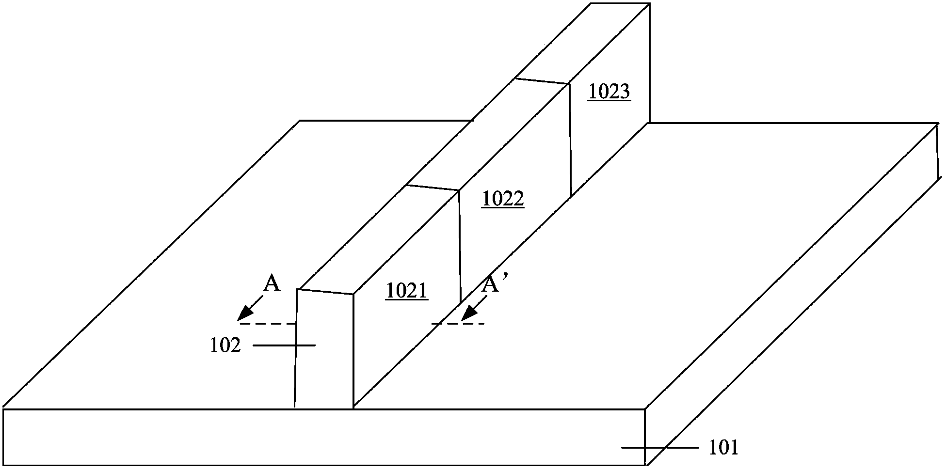
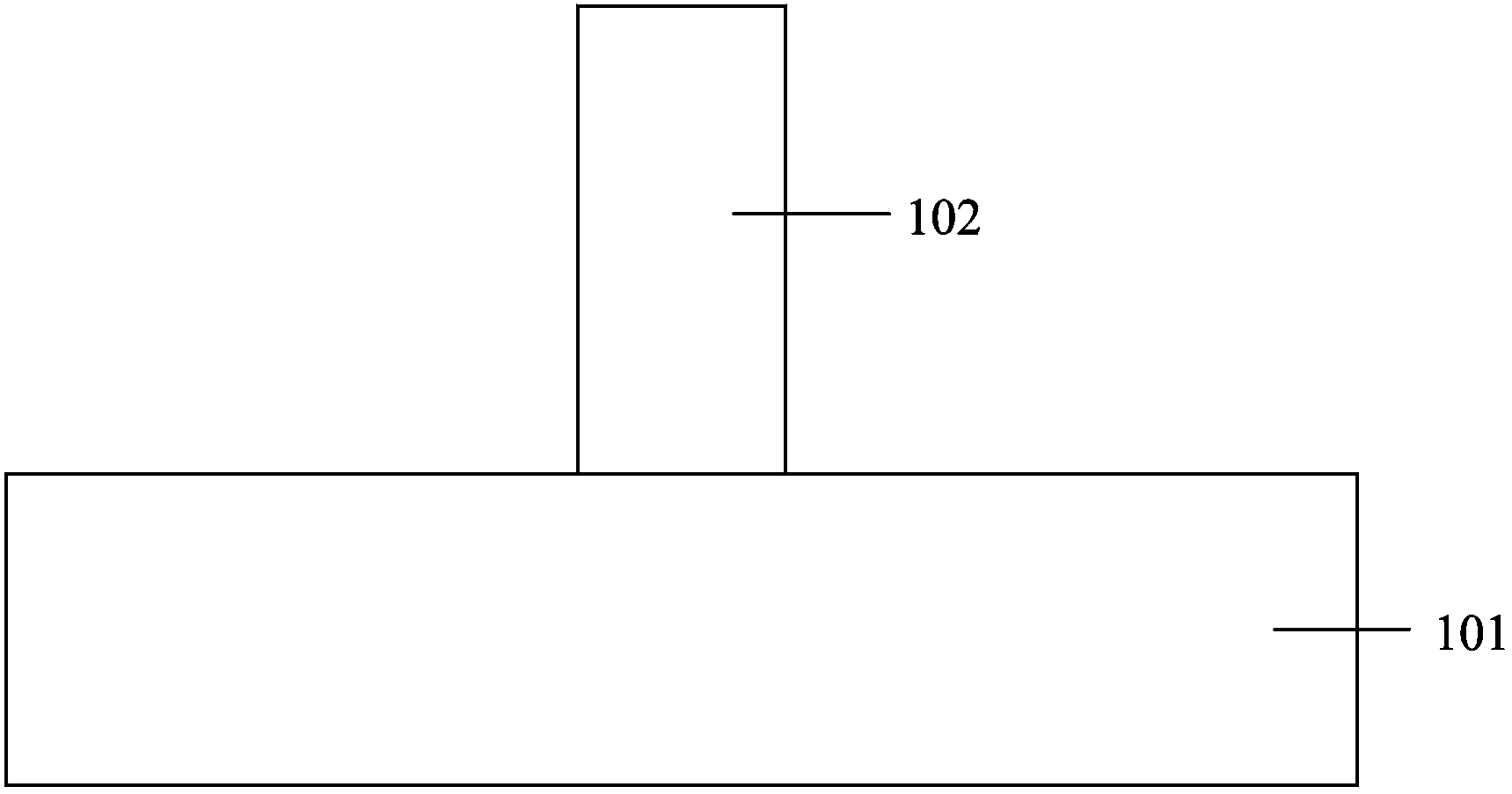
[0043] first reference Figures 4A-4C , providing a base 201 ; forming a fin doped with impurities on the base 201 as a first region 202 .
[0044] Figure 4A It is a schematic diagram of the three-dimensional structure of fins formed on the base 201, Figure 4B for Figure 4A The sectional view of the plane cut by the median line A-A', Figure 4C for Figure 4A Sectional view of the plane cut by the median line B-B'.
[0045] In a specific embodiment, the material of the substrate 201 may be silicon, silicon germanium, silicon on...
no. 2 Embodiment
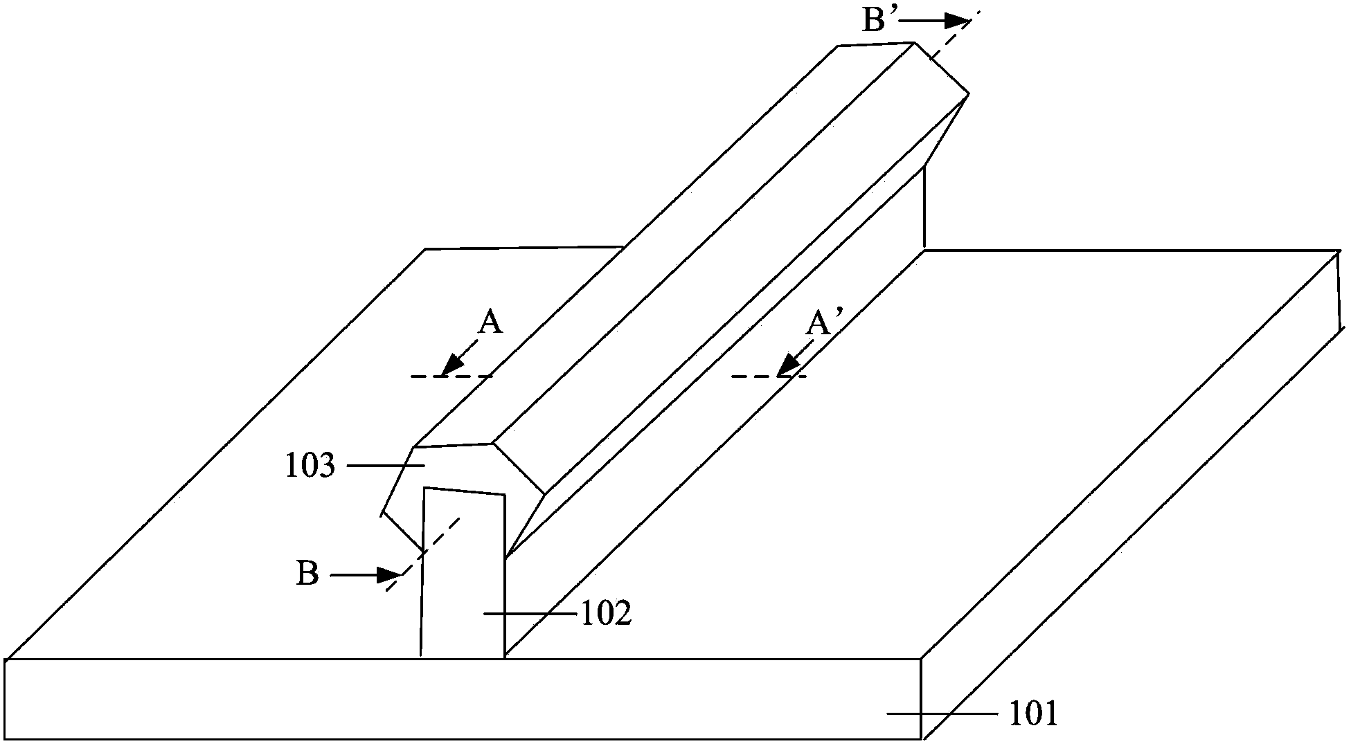
[0068] refer to Figures 8A-8C The difference between the second specific embodiment and the first specific embodiment is that: a second region 204 is formed in the base region 203 . For others, reference may be made to the first specific embodiment, and details are not repeated here.
[0069] In a specific embodiment, the doping depth H2 in the base region 203 is smaller than the height H1 of the base region 203 higher than the first region 202 , so as to prevent the first region 202 from contacting the second region 204 .
[0070] Figure 8A It is a schematic diagram of the three-dimensional structure of the second region 204 formed in the base region 203, Figure 8B for Figure 8A The sectional view of the plane cut by the median line A-A', Figure 8C for Figure 8A Sectional view of the plane cut by the median line B-B'. refer to Figure 8B , in this embodiment, the doping depth H2 is smaller than the height H1 of the base region 203 higher than the first region 202...
no. 3 Embodiment
[0073] This embodiment is an embodiment of a fin bipolar junction transistor.
[0074] refer to Figures 6A-6C The fin bipolar junction transistor includes: a base 201; a fin doped with impurities on the base 201, and the fin is a first region 202;
[0075] a base area 203 located on the first area 202;
[0076] The second region 204 located on the base region 203 . The first region 202 is an emission region, and the second region 204 is a collector region; or the first region 202 is a collector region, and the second region 204 is an emission region. The doping type of the base region 203 is opposite to that of the first region 202 , and the doping type of the second region 204 is the same as that of the first region 202 .
[0077] refer to Figure 6C , in a specific embodiment, the length L2 of the base region 203 is smaller than the length L1 of the first region 202 .
[0078] In a specific example, refer to Figure 6C , the length L3 of the second region 204 is small...
PUM
 Abstract
Description
Claims
Application Information
 - R&D
- Intellectual Property
- Life Sciences
- Materials
- Tech Scout
- Unparalleled Data Quality
- Higher Quality Content
- 60% Fewer Hallucinations
Browse by: Latest US Patents, China's latest patents, Technical Efficacy Thesaurus, Application Domain, Technology Topic, Popular Technical Reports.
© 2025 PatSnap. All rights reserved.Legal|Privacy policy|Modern Slavery Act Transparency Statement|Sitemap|About US| Contact US: help@patsnap.com