Shift register, gate drive circuit and display device
A shift register and gate technology, applied in static memory, digital memory information, instruments, etc., can solve the problems of difficult application and high production cost, and achieve the effect of reducing production cost and improving product competitiveness
- Summary
- Abstract
- Description
- Claims
- Application Information
AI Technical Summary
Problems solved by technology
Method used
Image
Examples
example 1
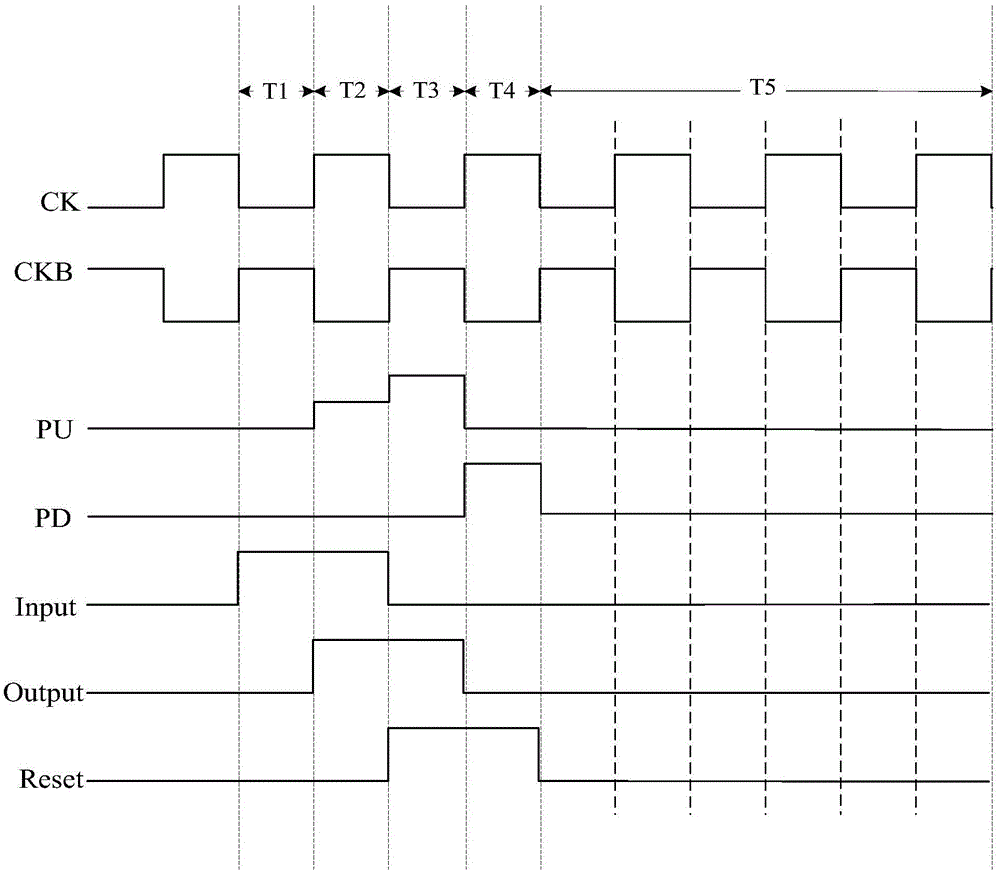
[0102] by Figure 4a The input-output timing diagram shown is an example for Figure 3a The working process of the shift register shown is described, specifically, select as Figure 4a There are five stages T1-T5 in the input and output sequence diagram shown.
[0103] In the T1 stage, Input=1, Reset=0, CK=0, CKB=1. Since Input=1, the first transistor T1, the third transistor T3, the fifth transistor T5 and the seventh transistor T7 are turned on, the signal of the pull-down node PD is a low potential pull-up signal, and the eighth transistor T8 is turned off; because Reset=0 , so the fourth transistor T4 and the sixth transistor T6 are turned off; since CK=0, the potential at point A is low, the second transistor T2 is turned off, and the signal of the pull-up node PU is a low-potential pull-up signal; since the pull-up node The signal of PU is a low-potential pull-up signal, so the tenth transistor T10 and the twelfth transistor T12 are turned off; since the signal of the...
example 2
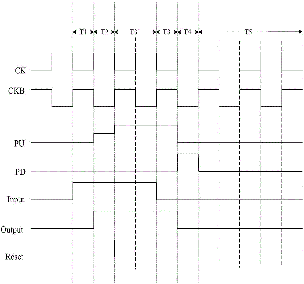
[0109] by Figure 4b The input-output timing diagram shown is an example for Figure 3a The working process of the shift register shown is described, specifically, select as Figure 4b There are five stages T1, T2, T3', T4 and T5 in the input and output timing diagram shown.
[0110] In the T1 stage, Input=1, Reset=0, CK=0, CKB=1. The specific working process is the same as the T1 stage in Example 1.
[0111] In the T2 stage, Input=1, Reset=0, CK=1, CKB=0. The specific working process is the same as the T2 stage in Example 1.
[0112]In the T3' phase, Input=1, Reset=1. Since Input=1, the first transistor T1, the third transistor T3, the fifth transistor T5 and the seventh transistor T7 are turned on; because Reset=1, the fourth transistor T4 and the sixth transistor T6 are turned on; because the third transistor T3, the fourth transistor T4, and the fifth transistor T5 are all turned on, and CK and CKB work together, so whether it is in the stage of CK=1, CKB=0, or in th...
PUM
 Abstract
Description
Claims
Application Information


