
Signal transmission circuit suitable for DDR (Double Date Rate Synchronous Dynamic Random Access Memory)

A signal transmission and circuit technology, applied in the direction of logic circuit coupling/interface, logic circuit, logic circuit connection/interface arrangement using field effect transistors, etc., can solve problems such as signal instability

Inactive Publication Date: 2014-11-05
MEDIATEK INC
View PDF7 Cites 10 Cited by
  • Summary
  • Abstract
  • Description
  • Claims
  • Application Information

AI Technical Summary

Problems solved by technology

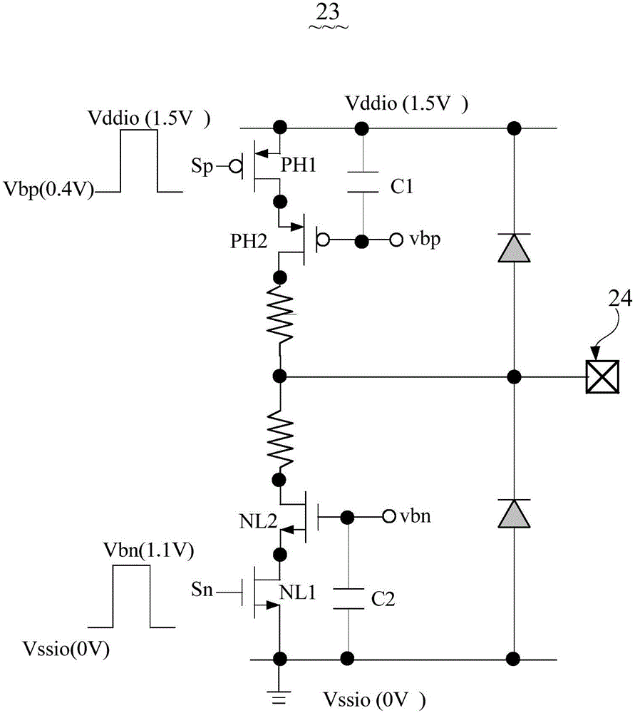
[0007] However, in the output circuit 23, the parasitic capacitance between the gate of the pull-up transistor PMOS PH2 and the pull-down transistor NOMS NL2 and the connection pad 24 is very large, so in order to avoid the signal change on the connection pad 24, due to capacitive coupling The signals of the received reference voltages Vbp and Vbn on the gates of the pull-up transistor PMOS PH2 and the pull-down transistor NOMS NL2 are not stable, so it is necessary to connect a relatively large The decoupling capacitors C1 and C2 are used to eliminate and reduce the influence of signal changes on the connection pad 24 on the reference voltages Vbp and Vbn, and the semiconductor area occupied by the decoupling capacitors C1 and C2 will also be very considerable

Method used


Image

  • Signal transmission circuit suitable for DDR (Double Date Rate Synchronous Dynamic Random Access Memory)
  • Signal transmission circuit suitable for DDR (Double Date Rate Synchronous Dynamic Random Access Memory)
  • Signal transmission circuit suitable for DDR (Double Date Rate Synchronous Dynamic Random Access Memory)

Examples


Embodiment Construction

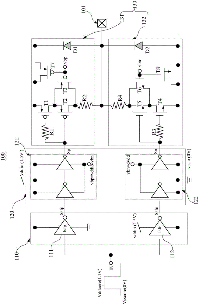
[0027] see image 3 , which is a schematic diagram of a signal transmission circuit suitable for DDR shown in an embodiment of the present invention. Here, DDR3 is taken as an example to introduce the present invention, and its operating voltage is 1.5V. Of course, the present invention is not limited thereto, and it can also be applied to other types of DDR, such as DDR3L with an operating voltage of 1.35V or an operating voltage of 1.35V. 1.2V DDR4.

[0028] Such as image 3 As shown, the signal transmission circuit 100 of the present invention is used to drive the connection pad 101 , which includes a level shift circuit 110 , a buffer circuit 120 and an output circuit 130 .

[0029] The level shifter circuit 110 includes an upper level shifter 111 and a lower level shifter 112, wherein the upper level shifter 111 and the lower level shifter 112 are respectively set at the operating voltage Vddio (1.5V) and ground voltage of DDR3 between Vssio(0V). And the upper level s...


PUM


Abstract

The invention discloses a signal transmission circuit suitable for a DDR (Double Date Rate Synchronous Dynamic Random Access Memory). The signal transmission circuit is used for driving a connection pad, and consists of a level shifting circuit which comprises upper and lower lever shifters, a buffer circuit which comprises upper and lower buffer units, and an output circuit which comprises a pull-up circuit and a pull-down circuit, wherein the upper level shifter and the lower level shifter are arranged between the operating voltage of the DDR and the ground voltage, and are used for receiving an input signal which comprises a first working voltage and a second working voltage; the first working voltage is equal to the ground voltage; the second working voltage is smaller than the operating voltage of the DDR; the upper buffer unit is arranged between the operating voltage of the DDR and a first reference voltage; the lower buffer unit is arranged between the ground voltage and a second reference voltage; the upper level shifter and the lower level shifter are input / output devices for outputting a first offset signal and a second offset signal which correspond to each other, and other elements are core devices; the second reference voltage is equal to the second working voltage; and the first reference voltage is equal to a difference value obtained by subtracting the second reference voltage from the operating voltage of the DDR.

Description

technical field [0001] The invention relates to a signal transmission circuit, in particular to a signal transmission circuit suitable for DDR. Background technique [0002] The full name of DDR is DDR SDRAM (Double Date Rate Synchronous Dynamic Random Access Memory, double rate synchronous dynamic random access memory). DDR was first proposed by Samsung in 1996. It is a memory specification agreed by eight companies including NEC, Mitsubishi, Fujitsu, Toshiba, Hitachi, Texas Instruments, Samsung and Hyundai, and has been approved by major chipset manufacturers such as AMD, VIA and SiS. support. DDR is an upgraded version of ordinary SDRAM, so it is also called SDRAM II. The most important change in DDR technology is in data transmission. It can transmit data on both the rising and falling edges of the clock, so it can double the data transmission rate while keeping the clock rate constant. Therefore, DDR is widely used. It is used in various signal processing systems. ...

Claims


Application Information

Patent Timeline
Patent Type & Authority Applications(China)
IPC IPC(8): H03K19/0185
CPCH03K19/018521G11C7/1057G11C7/225
Inventor 张耀忠许健丰
Owner MEDIATEK INC
Learn More