Array substrate, driving method of array substrate and display device

An array substrate and substrate technology, which can be used in static indicators, instruments, electrical and digital data processing, etc., and can solve problems such as cumbersome and inconvenient

Active Publication Date: 2014-11-19
BOE TECH GRP CO LTD +1
View PDF6 Cites 110 Cited by
  • Summary
  • Abstract
  • Description
  • Claims
  • Application Information

AI Technical Summary

Problems solved by technology

[0004] At present, the fingerprint identification module is usually installed in a vacant position outside the display area of ​​the mobile media to realize the fingerprint identification function. When users use it, they generally need to perform fingerprint identification before operating, which is not convenient enough, and it is necessary to combine the display device and the fingerprint identification device during manufacturing. Combining functions is relatively cumbersome

Method used


Image

  • Array substrate, driving method of array substrate and display device
  • Array substrate, driving method of array substrate and display device
  • Array substrate, driving method of array substrate and display device

Examples


Embodiment 1

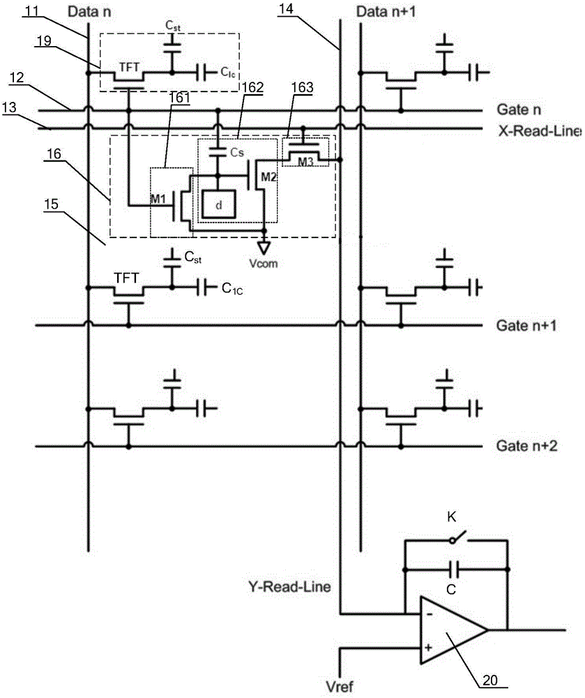
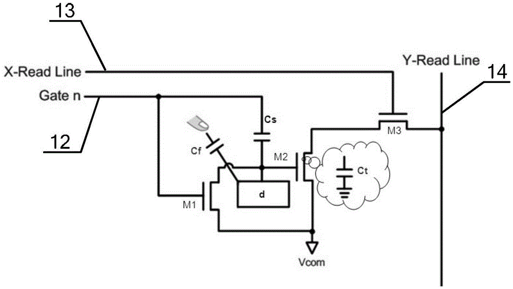
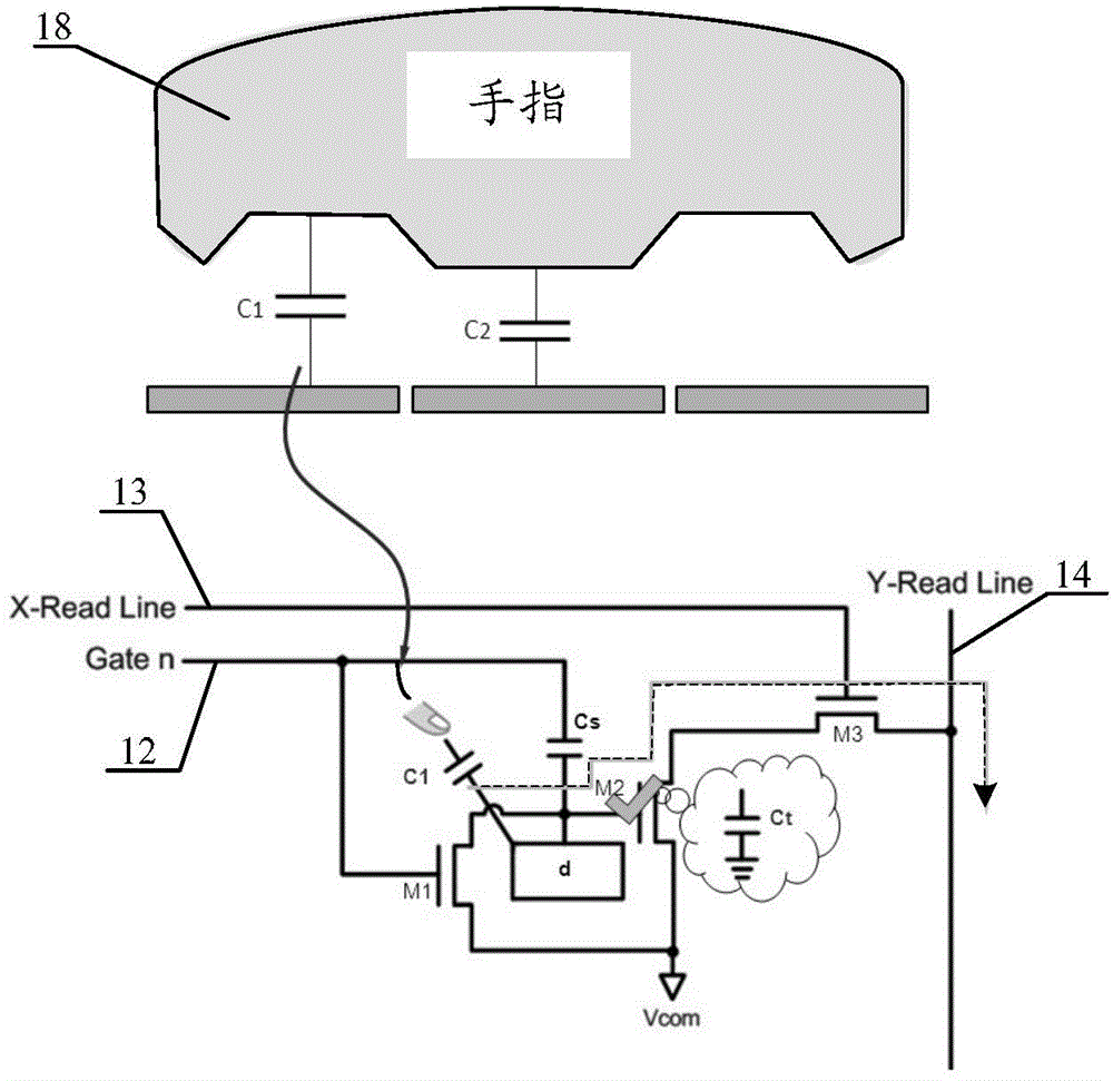
[0052] An embodiment of the present invention provides an array substrate, referring to figure 1 As shown, the array substrate includes a base, on which are formed data lines 11 and gate lines 12, and pixel units 15 defined by the data lines 11 and gate lines 12, on which are also formed: a plurality of The fingerprint identification circuit 16 is built in the pixel unit 15 .

[0053] This embodiment provides a design scheme of an array substrate. The fingerprint identification circuit 16 is built into the pixel unit 15 of the display area, that is, the pixel unit 15 is not only provided with a pixel display circuit 19, but also provided with a fingerprint identification circuit 16. Fingerprint identification and operation can be performed simultaneously during use, and the display device and the fingerprint identification device can be manufactured simultaneously without function combination, and the purpose of simplifying operation and manufacturing process can be achieved. ...

Embodiment 2

[0078] The embodiment of the present invention also provides another array substrate, which is different from the array substrate described in Embodiment 1 in that, as Figure 7 As shown, the base of the array substrate is further formed with: a plurality of light-sensing touch circuits 17 for realizing the light-sensing touch function, and the light-sensing touch circuits 17 are also built into the pixel unit 15 .

[0079] The array substrate provided in this embodiment, in addition to the pixel display circuit 19 in each pixel, also includes a fingerprint recognition circuit 16 and a light-sensitive touch circuit 17 built in the pixel unit 15, and the fingerprint recognition circuit 16 and the light-sensitive touch circuit 17 are both Introduced into the pixel unit 15 by periodic implantation, the fingerprint recognition circuit 16 and the light-sensitive touch circuit 17 can be located in the same pixel unit 15, or can be located in different pixel units 15, for example, as ...

Embodiment 3

[0099] An embodiment of the present invention also provides a display device, including the array substrate described in Embodiment 1 or Embodiment 2.

[0100] The array substrate in Embodiment 1 or Embodiment 2 introduces the fingerprint recognition function (or the fingerprint recognition function and the optical touch function together) into the display area, and the display panel using this array substrate can simultaneously realize the display and fingerprint recognition functions (or Fingerprint recognition and light-sensitive touch function). Using the display device with the above-mentioned array substrate, the user can simultaneously perform fingerprint recognition and operation when using it, and the display device and the fingerprint recognition device can be manufactured synchronously without functional combination, which can achieve the purpose of simplifying the operation and manufacturing process.

[0101] The display device may be any product or component with ...


PUM


Abstract

The embodiment of the invention discloses an array substrate, a driving method of the array substrate and a display device, and relates to the field of displaying. A fingerprint identification module can be arranged inside a display area, so that the purpose of simplifying operations and a manufacturing process is achieved. The array substrate comprises a substrate body, grid lines, data lines and pixel units defined by the grid lines and the data lines, the substrate body is also provided with a plurality of fingerprint identification circuits used for carrying out fingerprint identification, and the fingerprint identification circuits are arranged inside the pixel units.

Description

technical field [0001] The present invention relates to the display field, in particular to an array substrate, a driving method thereof, and a display device. Background technique [0002] Recently, with the rise of mobile media such as mobile phones and tablets, consumers are increasingly demanding personal data security. At the same time, the convenience of operation and the diversity of applications are also one of the key points that designers need to consider. [0003] In the security-based personal verification system, the fingerprint recognition method using a fingerprint recognition device has been widely used, because the fingerprint recognition method can be implemented at a very low cost and has the characteristics of high usability and high accuracy. At present, the fingerprint identification device is mainly based on semiconductor silicon capacitance effect (using silicon sensor to identify fingerprint information), that is, the detection electrode of the silic...

Claims


Application Information

Patent Timeline
Patent Type & Authority Applications(China)
IPC IPC(8): G02F1/133
CPCG06F3/042G06F2203/04103G09G3/3648G06F3/0412G06F3/0443G06F3/04166G06V40/1318G06V40/1306
Inventor 杨盛际董学王海生刘英明刘红娟
Owner BOE TECH GRP CO LTD
Why Eureka
Try Eureka