Manufacturing method of tunable semiconductor laser and tunable semiconductor laser

A manufacturing method and laser technology, which are applied to semiconductor lasers, optical waveguide semiconductor structures, lasers, etc., can solve the problems of laser performance impact and laser manufacturing technology differences, so as to reduce the number of device growth, shorten the research and development cycle, product high performance effects

Active Publication Date: 2008-07-23
GUANGXUN SCI & TECH WUHAN
View PDF2 Cites 38 Cited by
  • Summary
  • Abstract
  • Description
  • Claims
  • Application Information

AI Technical Summary

Problems solved by technology

Würzburg University and Max Planck Research Center in Germany reported DFB lasers for making vertical gratings in IEEE PHOTONICS TECHNOLOGY LETTERS, VOL.19, NO.5, P.264 in 2007, but they used dotted line quantum well technology, which is different from current practical lasers. Production techniques vary widely
And the grating is etched through the active area, and the lateral damage caused by the etching will also affect the performance of the laser
At present, vertical gratings are still only used in DFB lasers, and there are no related reports on DBR and SGDBR lasers.

Method used


Image

  • Manufacturing method of tunable semiconductor laser and tunable semiconductor laser
  • Manufacturing method of tunable semiconductor laser and tunable semiconductor laser
  • Manufacturing method of tunable semiconductor laser and tunable semiconductor laser

Examples


Embodiment Construction

[0043] The manufacturing method of the semiconductor laser and the semiconductor laser thereof of the present invention will be described in detail below with reference to the drawings and embodiments.

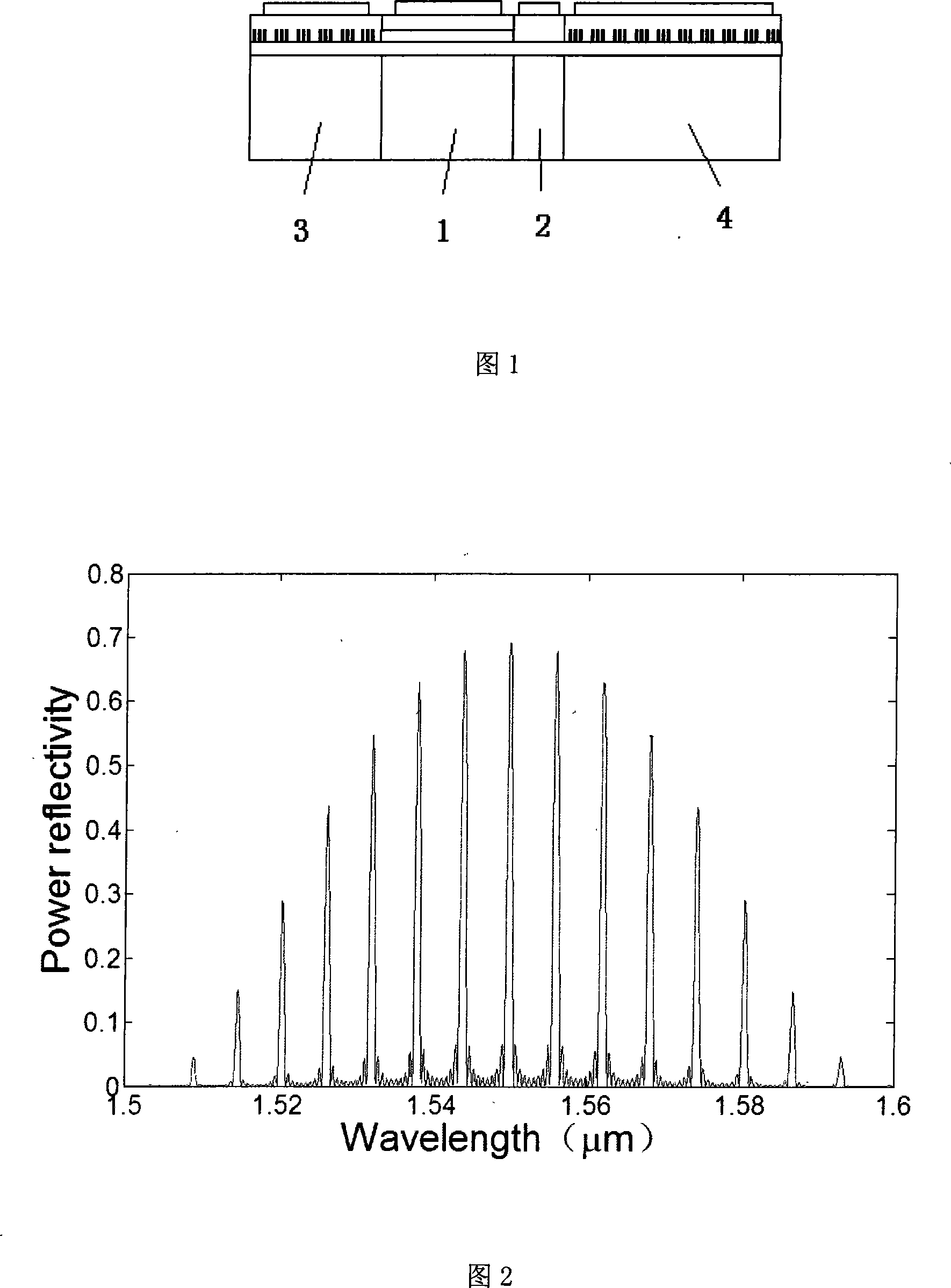
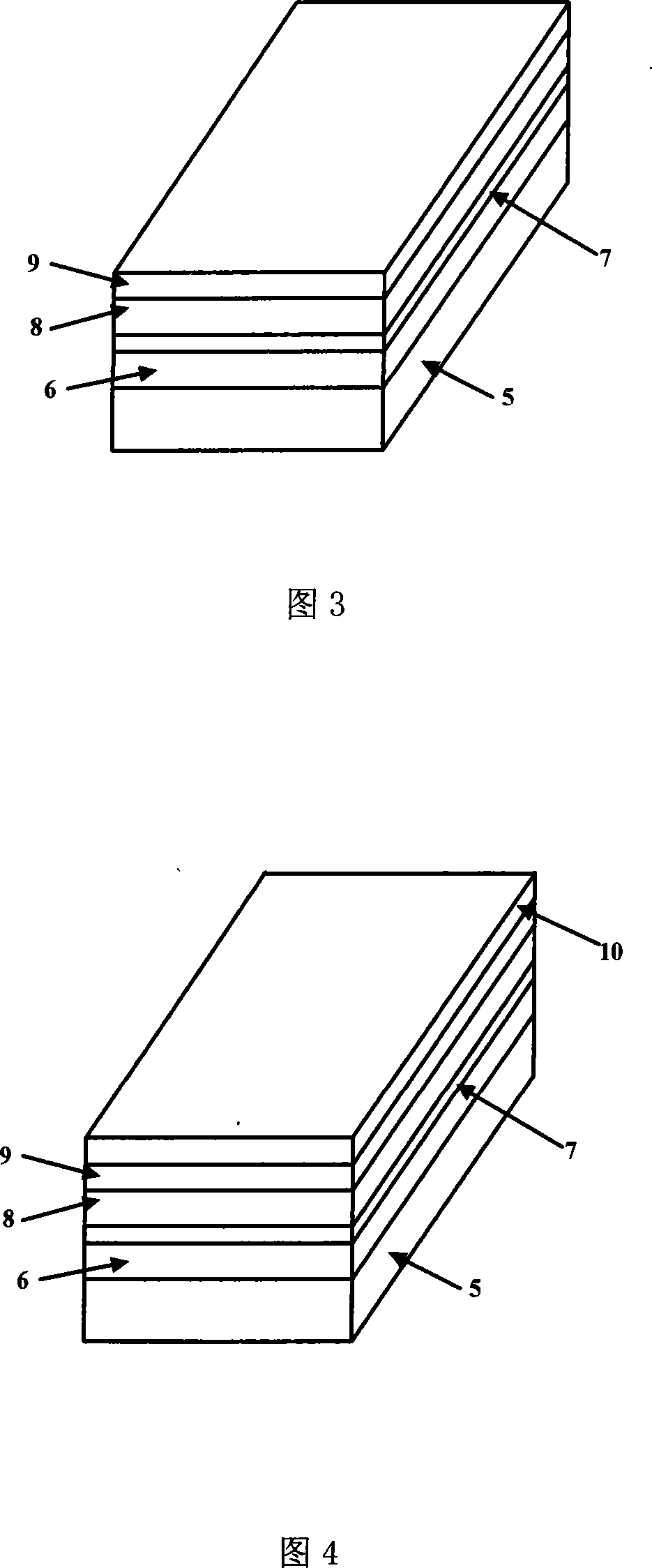
[0044]The fabrication method of the tunable semiconductor laser of the present invention comprises the following process steps (in conjunction with two-stage DBR):

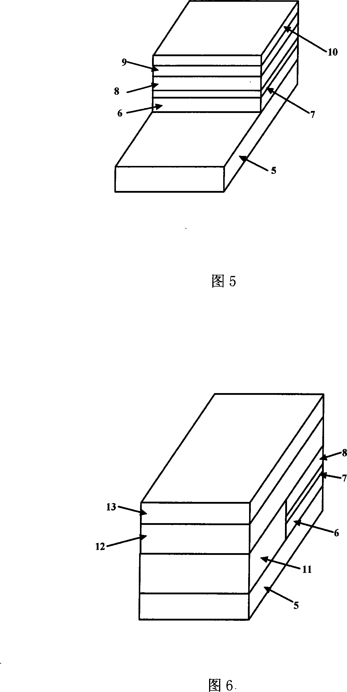
[0045] 1) As shown in Figure 3, epitaxial growth is performed on an n-type indium phosphide (InP) substrate 5, and the epitaxial layer structure from bottom to top is the lower waveguide layer 6, the multi-quantum well structure 7, the upper waveguide layer 8, and the phosphorus indium layer (InP) 9;

[0046] 2) As shown in FIG. 4, a silicon dioxide dielectric film 10 is grown on the epitaxial layer by using a plasma-enhanced chemical vapor deposition system (PECVD);

[0047] 3) As shown in Figure 5, the active waveguide area and the grating area (grating area) are divided into segmented graphics by photolithogra...


PUM


Abstract

Provided is a making method of a tunable semiconductor laser and a tunable semiconductor laser, wherein the making method comprises the following procedures: growing lower waveguide layer, multiple quantum trap structure, upper waveguide layer and indium phosphide layer epitaxially and sequentially on the n type substrate; growing earth silicon dielectric membrane on the epitaxial layer; dividing into active waveguide region and raster region; butting passive waveguide portion; removing earth silicon dielectric membrane and indium phosphide layer on the surface of the active waveguide region; growing ridge waveguide indium phosphide material and low resistivity InGaAs ternary layer sequentially; growing earth silicon dielectric membrane; making raster graphic of the ridge waveguide and the ridge waveguide on the raster region; etching raster of the ridge waveguide and the ridge waveguide on the raster region; growing earth silicon dielectric membrane continuously; opening the window separately on active waveguide region and raster region in order to make electrode isolation ditch; making P face and N face electrode of laser. The invention has good product property and high automation degree of the product making, which simplifies the technology process and has good product ratio.

Description

technical field [0001] The invention relates to a semiconductor laser for communication. In particular, it relates to a high-performance, high-automated manufacturing method of a distributed Bragg reflection and sampling grating distributed Bragg reflection tunable semiconductor laser and the tunable semiconductor laser. Background technique [0002] At present, there are many technologies for tunable lasers, mainly including vertical cavity surface emitting laser (VCSEL), external cavity tuning technology, distributed feedback Bragg laser (DFB) array technology, distributed Bragg reflection laser (DBR) and sampling grating distributed Bragg reflection. Laser (SGDBR) technology, etc. Among them, the output power of VCSEL is low, and due to the limitation of material properties, it is very difficult to develop in the long wavelength range (1310 to 1550nm); the external cavity tuning wavelength conversion speed is slow, and it depends on mechanical adjustment to tune the wave...

Claims


Application Information

Patent Timeline
Patent Type & Authority Applications(China)
IPC IPC(8): H01S5/12H01S5/125H01S5/10H01S5/22H01S5/34
Inventor 董雷张瑞康
Owner GUANGXUN SCI & TECH WUHAN
Why Eureka
Try Eureka