High-crystal-quality infrared light emitting diode
A technology of crystal quality and infrared luminescence, applied in semiconductor devices, electrical components, circuits, etc., can solve the problems of quantum well mismatch, poor crystal quality of epitaxial layers, etc., and achieve the effect of improving luminous efficiency
- Summary
- Abstract
- Description
- Claims
- Application Information
AI Technical Summary
Problems solved by technology
Method used
Image
Examples
Embodiment 1
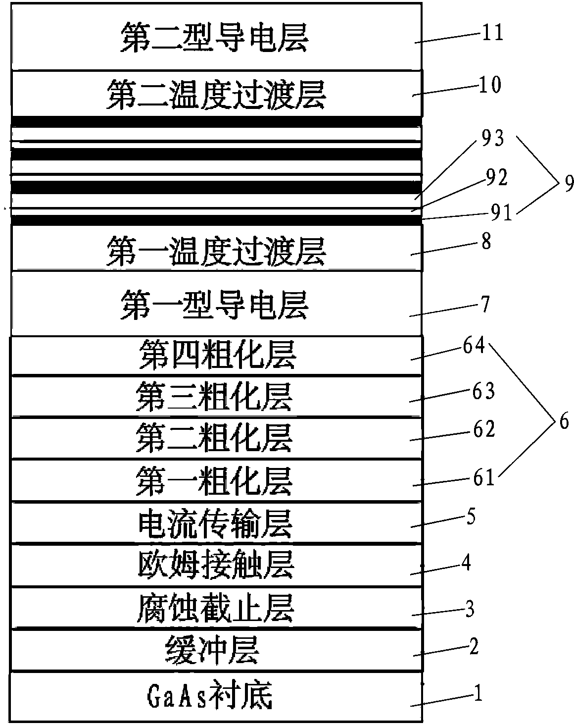
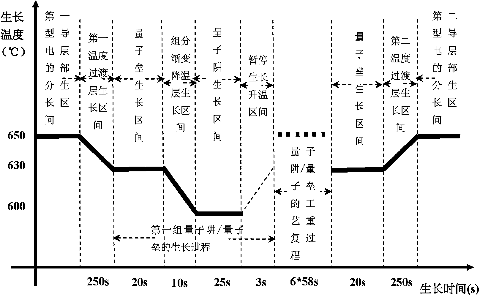
[0068] refer to Figure 1 to Figure 4 As shown, a high crystal quality infrared light-emitting diode disclosed by the present invention comprises growth buffer layer 2, corrosion stop layer 3, ohmic contact layer 4, current transport layer 5, and roughened layer 6 from substrate 1 to bottom to top. , the first type conduction layer 7 , the first temperature transition layer 8 , the active layer 9 , the second temperature transition layer 10 and the second type conduction layer 11 .
[0069] The roughened layer 6 is composed of four parts, namely a first roughened layer 61 , a second roughened layer 62 , a third roughened layer 63 , and a fourth roughened layer 64 .
[0070] The active layer 9 is composed of seven sets of quantum barriers 91 , composition gradient cooling layers 92 and quantum wells 93 alternately.
[0071] In order to achieve the preparation of infrared light-emitting diodes with high crystal quality, the following epitaxial growth steps are required:
[007...
Embodiment 2
[0091] The difference between the second embodiment and the first embodiment is that the active layer 9 is composed of six sets of quantum barriers 91 , composition gradient cooling layers 92 and quantum wells 93 alternately, while the first embodiment has seven sets.
[0092] Such as Figure 5 As shown, an infrared light-emitting diode, from the bottom to the top of the substrate 1 is a growth buffer layer 2, an etching stop layer 3, an ohmic contact layer 4, a current transmission layer 5, a roughening layer 6, and a first-type conductive layer 7 , a first temperature transition layer 8 , an active layer 9 , a second temperature transition layer 10 , and a second-type conductive layer 11 .
[0093] The roughened layer 6 is composed of four parts, namely the first roughened layer 61, the second roughened layer 62, the third roughened layer 63, and the fourth roughened layer 64; the active layer 9 consists of six groups of quantum barriers 91, Composition gradient cooling lay...
PUM
 Abstract
Description
Claims
Application Information


